|
Moteur de recherche de fiches techniques de composants électroniques |
|
|
Moteur de recherche de fiches techniques de composants électroniques |
|
EMC2104 Fiches technique(PDF) 80 Page - SMSC Corporation |
|
|
|||||||||||||||||||||||||||||
EMC2104 Fiches technique(HTML) 80 Page - SMSC Corporation |
|
|
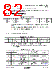
80 / 101 page  Dual RPM-Based PWM Fan Controller with Hardware Thermal Shutdown Datasheet Revision 1.74 (05-08-08) 80 SMSC EMC2104 DATASHEET 6.36 GPIO Direction Register The GPIO Direction Register 1 controls the direction of GPIOs 1 through 6. When muxable pins are not configured as a GPIO ports the respective bits are ignored. Bit 5 - 0 - GPIOx_DIR - Controls the input / output state of GPIOs. The bit is not used if the pin is not configured as a GPIO. ‘0’ (default) - The GPIO is configured as an input. ‘1’ - The GPIO is configured as an output. 6.37 GPIO / PWM Pin Output Configuration Register The GPIO Output Configuration Register controls the output pin type of each GPIO pin. These settings apply to the pin if it is configured as a GPIO output or a PWM. Bit 6 - PWM1_OT - Determines the output type for the PWM1 pin. ‘0’ (default) - The PWM1 output is configured as an open drain output (if enabled as a PWM output). ‘1’ - The PWM1 output is configured as a push-pull output (if enabled as an a PWM output). Bit 2 - 0 - GPIOx_OT - Determines the output type for GPIOx. ‘0’ (default) - GPIOx is configured as an open drain output (if enabled as an output). ‘1’ - GPIOxis configured as a push-pull output (if enabled as an output). 6.38 GPIO Input Register The GPIO Input Register indicates the state of the corresponding GPIO pin regardless of the functionality of the pin (GPIO, PWM, or TACH) or the direction of the GPIO (input, push-pull output, open-drain output). When a GPIO is configured as an input, any change of state will assert the ALERT# pin (unless GPIO interrupts are masked, see Section 6.15). Table 6.53 GPIO Direction Register ADDR R/W REGISTER B7B6 B5B4B3B2B1B0 DEFAULT E1h R/W GPIO Direction 1 --- -- GPIO 3_DIR GPIO 2_DIR GPIO 1_DIR 00h Table 6.54 GPIO / PWM Pin Output Configuration Register ADDR R/W REGISTER B7 B6 B5 B4 B3 B2 B1 B0 DEFAULT E2 R/W GPIO Output Config - PWM 1_OT --- GPIO 3_OT GPIO 2_OT GPIO 1_OT 00h Table 6.55 GPIO Input Register ADDR R/W REGISTER B7 B6 B5 B4 B3 B2 B1 B0 DEFAULT E3h R GPIO Input ---- - GPIO 3_IN GPIO 2_IN GPIO 1_IN 00h |
|
Lien URL |
| ALLDATASHEET vous a-t-il été utile ? [ DONATE ] |
À propos de Alldatasheet | Publicité | Contactez-nous | Politique de confidentialité | Lien vers la fiche technique | Echange de liens | Fabricants All Rights Reserved©Alldatasheet.com |
| Russian : Alldatasheetru.com | Korean : Alldatasheet.co.kr | Spanish : Alldatasheet.es | French : Alldatasheet.fr | Italian : Alldatasheetit.com Portuguese : Alldatasheetpt.com | Polish : Alldatasheet.pl | Vietnamese : Alldatasheet.vn Indian : Alldatasheet.in | Mexican : Alldatasheet.com.mx | British : Alldatasheet.co.uk | New Zealand : Alldatasheet.co.nz |
|
Family Site : ic2ic.com |
icmetro.com |
 French ▼
 English
 Chinese
 German
 Japanese
 Russian
 Korean
 Spanish
 French
 Italian
 Portuguese
 Polish
 Vietnamese
 Indian
 Mexican
 British
 New Zealand