|
Moteur de recherche de fiches techniques de composants électroniques |
|
|
Moteur de recherche de fiches techniques de composants électroniques |
|
L99MM70XP Fiches technique(PDF) 10 Page - STMicroelectronics |
|
|
|||||||||||||||||||||||||||||
L99MM70XP Fiches technique(HTML) 10 Page - STMicroelectronics |
|
|
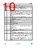
10 / 68 page  Pin definitions and functions L99MM70XP 10/68 Doc ID 022637 Rev 2 16 VS (Reg) Power supply voltage (external reverse protection required): for this input a ceramic capacitor as close as possible to GND and an electrolytic capacitor to buffer the voltage during negative transients is recommended. 17 LIN LIN bus line 23 OUT6 High-side driver output 6: The output is built by a high-side switch and is intended for resistive loads; hence the internal reverse diode from GND to the output is missing. For ESD reason a diode to GND is present but the energy which can be dissipated is limited. The high-side driver is a power DMOS transistor with an internal parasitic reverse diode from the output to VS (bulk-drain-diode). The output is overcurrent and open-load protected. 24 INH/PWM3 Inhibit input: wake-up from external CAN transceiver. This pin has a second functionality. The microcontroller can use the INH signal to provide a third PWM input for the output OUT8. 25 CP Charge pump output: This output is provided to drive the gate of an external n-channel power MOS used for reverse polarity protection (see Figure 1). 26 PWM1 PWM1 input: This input signal can be used to control the drivers OUT1-OUT5, OUT7, and OUT9 by an external PWM signal. 27 NRES Low active reset output to the microcontroller: internal pull up of typ. 100k 28 PWM2 PWM2 input: This input signal can be used to control the driver OUT6 by an external PWM signal. 29 ECDR ECDR: using the device in EC control mode this pin is used to control the gate of an external MOSFET. 30 OUT8 High-side driver output 8: see OUT6 Note: This output can be configured to supply a bulb with low on-resistance or a LED with higher on-resistance in a different application. 31 OUT7/EC High-side driver output 7: see OUT6 Note: Beside the bit 8 in control register 2 this output can be switched on setting bit 0 for electrochrome control mode with higher priority. 33 ECFD ECFD: using the device in EC control mode this pin is used as “virtual GND” for the EC-glass. For EC-glasses, that require a negative discharge voltage, this supplies the fast discharge voltage. If no EC-glass is used, this pin must be connected to ground. 34 ECV ECV: Using the device in EC control mode this pin is used as voltage monitor input. For fast discharge an additional low-side-switch is implemented. This pin can be used as “stand alone” low-side as well. This output is intended for resistive loads only Table 2. Pin definition and functions (continued) Pin Symbol Function |
|
Lien URL |
| ALLDATASHEET vous a-t-il été utile ? [ DONATE ] |
À propos de Alldatasheet | Publicité | Contactez-nous | Politique de confidentialité | Lien vers la fiche technique | Echange de liens | Fabricants All Rights Reserved©Alldatasheet.com |
| Russian : Alldatasheetru.com | Korean : Alldatasheet.co.kr | Spanish : Alldatasheet.es | French : Alldatasheet.fr | Italian : Alldatasheetit.com Portuguese : Alldatasheetpt.com | Polish : Alldatasheet.pl | Vietnamese : Alldatasheet.vn Indian : Alldatasheet.in | Mexican : Alldatasheet.com.mx | British : Alldatasheet.co.uk | New Zealand : Alldatasheet.co.nz |
|
Family Site : ic2ic.com |
icmetro.com |
 French ▼
 English
 Chinese
 German
 Japanese
 Russian
 Korean
 Spanish
 French
 Italian
 Portuguese
 Polish
 Vietnamese
 Indian
 Mexican
 British
 New Zealand