|
Moteur de recherche de fiches techniques de composants électroniques |
|
|
Moteur de recherche de fiches techniques de composants électroniques |
|
ST10F269Z1Q6 Fiches technique(PDF) 17 Page - STMicroelectronics |
|
|
|||||||||||||||||||||||||||||
ST10F269Z1Q6 Fiches technique(HTML) 17 Page - STMicroelectronics |
|
|
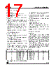
17 / 184 page  ST10F269 5 - INTERNAL FLASH MEMORY 17/184 5 - INTERNAL FLASH MEMORY 5.1 - Overview – 128K or 256K Byte on-chip Flash memory – Two possibilities of Flash mapping into the CPU address space – Flash memory can be used for code and data storage – 32-bit, zero waitstate read access (50ns cycle time at fCPU = 40MHz on PQFP144 devices and 62.5ns cycle time at fCPU = 32MHz on TQFP144 devices) – Erase-Program Controller (EPC) similar to M29F400B STM’s stand-alone Flash memory • Word-by-Word Programmable (16 µs typical) • Data polling and Toggle Protocol for EPC Status • Ready/Busy signal connected on XP2INT interrupt line • Internal Power-On detection circuit – Memory Erase in blocks • One 16K Byte, two 8K Byte, one 32K Byte, one to three 64K Byte blocks • Each block can be erased separately (1.5 second typical) • Chip erase (8.5 second typical) • Each block can be separately protected against programming and erasing • Each protected block can be temporary unpro- tected • When enabled, the read protection prevents access to data in Flash memory using a pro- gram running out of the Flash memory space. Access to data of internal Flash can only be per- formed with an inner protected program – Erase Suspend and Resume Modes • Read and Program another Block during erase suspend – Single Voltage operation, no need of dedicated supply pin – Low Power Consumption: • 45mA max. Read current • 60mA max. Program or Erase current • Automatic Stand-by-mode (50 µA maximum) – 1000 Erase-Program Cycles per block, 20 years of data retention time – Operating temperature: -40 to +125oC / -40 to +125oC 5.2 - Operational Overview Read Mode In standard mode (the normal operating mode) the Flash appears like an on-chip ROM with the same timing and functionality. The Flash module offers a fast access time, allowing zero waitstate access with CPU frequency up to 40MHz on PQFP144 devices and up to 32MHz on TQFP144 devices. Instruction fetches and data operand reads are performed with all addressing modes of the ST10F269 instruction set. In order to optimize the programming time of the internal Flash, blocks of 8K Bytes, 16K Bytes, 32K Bytes, 64K Bytes can be used. But the size of the blocks does not apply to the whole memory space, see details in Table 2. *Not available on 128K versions (reserved areas). Table 2 : 128K or 256K Byte Flash Memory Block Organization Block Addresses (Segment 0) Addresses (Segment 1) Size (byte) 0 1 2 3 4 5* 6* 00’0000h to 00’3FFFh 00’4000h to 00’5FFFh 00’6000h to 00’7FFFh 01’8000h to 01’FFFFh 02’0000h to 02’FFFFh 03’0000h to 03’FFFFh* 04’0000h to 04’FFFFh* 01’0000h to 01’3FFFh 01’4000h to 01’5FFFh 01’6000h to 01’7FFFh 01’8000h to 01’FFFFh 02’0000h to 02’FFFFh 03’0000h to 03’FFFFh* 04’0000h to 04’FFFFh* 16K 8K 8K 32K 64K 64K* 64K* |
|
Lien URL |
| ALLDATASHEET vous a-t-il été utile ? [ DONATE ] |
À propos de Alldatasheet | Publicité | Contactez-nous | Politique de confidentialité | Lien vers la fiche technique | Echange de liens | Fabricants All Rights Reserved©Alldatasheet.com |
| Russian : Alldatasheetru.com | Korean : Alldatasheet.co.kr | Spanish : Alldatasheet.es | French : Alldatasheet.fr | Italian : Alldatasheetit.com Portuguese : Alldatasheetpt.com | Polish : Alldatasheet.pl | Vietnamese : Alldatasheet.vn Indian : Alldatasheet.in | Mexican : Alldatasheet.com.mx | British : Alldatasheet.co.uk | New Zealand : Alldatasheet.co.nz |
|
Family Site : ic2ic.com |
icmetro.com |
 French ▼
 English
 Chinese
 German
 Japanese
 Russian
 Korean
 Spanish
 French
 Italian
 Portuguese
 Polish
 Vietnamese
 Indian
 Mexican
 British
 New Zealand