|
Moteur de recherche de fiches techniques de composants électroniques |
|
|
Moteur de recherche de fiches techniques de composants électroniques |
|
ST10F269Z1Q6 Fiches technique(PDF) 93 Page - STMicroelectronics |
|
|
|||||||||||||||||||||||||||||
ST10F269Z1Q6 Fiches technique(HTML) 93 Page - STMicroelectronics |
|
|
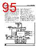
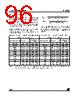
93 / 184 page  ST10F269 13 - A/D CONVERTER 93/184 13 - A/D CONVERTER A 10-bit A/D converter with 16 multiplexed input channels and a sample and hold circuit is integrated on-chip. The sample time (for loading the capacitors) and the conversion time is programmable and can be adjusted to the external circuitry. To remove high frequency components from the analog input signal, a low-pass filter must be con- nected at the ADC input. Overrun error detection / protection is controlled by the ADDAT register. Either an interrupt request is generated when the result of a previous conversion has not been read from the result register at the time the next conversion is complete, or the next conversion is suspended until the previous result has been read. For applications which require less than 16 analog input channels, the remaining channel inputs can be used as digital input port pins. The A/D converter of the ST10F269 supports different conversion modes: – Single channel single conversion: the analog level of the selected channel is sampled once and converted. The result of the conversion is stored in the ADDAT register. – Single channel continuous conversion: the analog level of the selected channel is repeated- ly sampled and converted. The result of the con- version is stored in the ADDAT register. – Auto scan single conversion: the analog level of the selected channels are sampled once and converted. After each conversion the result is stored in the ADDAT register. The data can be transferred to the RAM by interrupt software management or using the powerful Peripheral Event Controller (PEC) data transfer. – Auto scan continuous conversion: the analog level of the selected channels are repeatedly sampled and converted. The result of the con- version is stored in the ADDAT register. The data can be transferred to the RAM by interrupt software management or using the PEC data transfer. – Wait for ADDAT read mode: when using con- tinuous modes, in order to avoid to overwrite the result of the current conversion by the next one, the ADWR bit of ADCON control register must be activated. Then, until the ADDAT regis- ter is read, the new result is stored in a tempo- rary buffer and the conversion is on hold. – Channel injection mode: when using continuous modes, a selected channel can be converted in between without changing the current operating mode. The 10-bit data of the conversion are stored in ADRES field of ADDAT2. The current continuous mode remains active after the single conversion is completed Notes: 1. Section 21.4.5 -: Direct Drive for TCL definition. 2. tCC = TCL x 24 Table 26 : ADC Sample Clock and Conversion Clock (PQFP144 devices) ADCTC Conversion Clock tCC ADSTC Sample Clock tSC TCL1 = 1/2 x fXTAL At fCPU = 40MHz tSC =At fCPU = 40MHz 00 TCL x 24 0.3 µs00 tCC 0.3 µs 2 01 Reserved, do not use Reserved 01 tCC x 2 0.6 µs 2 10 TCL x 96 1.2 µs10 tCC x 4 1.2 µs 2 11 TCL x 48 0.6 µs11 tCC x 8 2.4 µs 2 |
|
Lien URL |
| ALLDATASHEET vous a-t-il été utile ? [ DONATE ] |
À propos de Alldatasheet | Publicité | Contactez-nous | Politique de confidentialité | Lien vers la fiche technique | Echange de liens | Fabricants All Rights Reserved©Alldatasheet.com |
| Russian : Alldatasheetru.com | Korean : Alldatasheet.co.kr | Spanish : Alldatasheet.es | French : Alldatasheet.fr | Italian : Alldatasheetit.com Portuguese : Alldatasheetpt.com | Polish : Alldatasheet.pl | Vietnamese : Alldatasheet.vn Indian : Alldatasheet.in | Mexican : Alldatasheet.com.mx | British : Alldatasheet.co.uk | New Zealand : Alldatasheet.co.nz |
|
Family Site : ic2ic.com |
icmetro.com |
 French ▼
 English
 Chinese
 German
 Japanese
 Russian
 Korean
 Spanish
 French
 Italian
 Portuguese
 Polish
 Vietnamese
 Indian
 Mexican
 British
 New Zealand