|
Moteur de recherche de fiches techniques de composants électroniques |
|
|
Moteur de recherche de fiches techniques de composants électroniques |
|
ST10F269Z1Q6 Fiches technique(PDF) 57 Page - STMicroelectronics |
|
|
|||||||||||||||||||||||||||||
ST10F269Z1Q6 Fiches technique(HTML) 57 Page - STMicroelectronics |
|
|
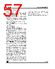
57 / 184 page  ST10F269 12 - PARALLEL PORTS 57/184 12 - PARALLEL PORTS 12.1 - Introduction The ST10F269 MCU provides up to 111 I/O lines with programmable features. These capabilities bring very flexible adaptation of this MCU to wide range of applications. ST10F269 has 9 groups of I/O lines gathered as following: – Port 0 is a 2 time 8-bit port named P0L (Low as less significant Byte) and P0H (high as most sig- nificant Byte) – Port 1 is a 2 time 8-bit port named P1L and P1H – Port 2 is a 16-bit port – Port 3 is a 15-bit port (P3.14 line is not imple- mented) – Port 4 is a 8-bit port – Port 5 is a 16-bit port input only – Port 6, Port 7 and Port 8 are 8-bit port These ports may be used as general purpose bidirectional input or output, software controlled with dedicated registers. For example the output drivers of six of the ports (2, 3, 4, 6, 7, 8) can be configured (bit-wise) for push-pull or open drain operation using ODPx registers. In addition, the sink and the source capability and the rise / fall time of the transition of the signal of some of the push-pull buffers can be programmed to fit the driving requirements of the application and to minimize EMI. This feature is implemented on Port 0, 1, 2, 3, 4, 6, 7 and 8 with the control registers POCONx. The output drivers capabilities of ALE, RD, WR control lines are programmable with the dedicated bits of POCON20 control register. The input threshold levels are programmable (TTL/CMOS) for 5 ports (2, 3, 4, 7, 8). The logic level of a pin is clocked into the input latch once per state time, regardless whether the port is configured for input or output. The threshold is selected with the PICON register control bits. A write operation to a port pin configured as an input causes the value to be written into the port output latch, while a read operation returns the latched state of the pin itself. A read-modify-write operation reads the value of the pin, modifies it, and writes it back to the output latch. Writing to a pin configured as an output (DPx.y=‘1’) causes the output latch and the pin to have the written value, since the output buffer is enabled. Reading this pin returns the value of the output latch. A read-modify-write operation reads the value of the output latch, modifies it, and writes it back to the output latch, thus also modifying the level at the pin. I/O lines support an alternate function which is detailed in the following description of each port. |
|
Lien URL |
| ALLDATASHEET vous a-t-il été utile ? [ DONATE ] |
À propos de Alldatasheet | Publicité | Contactez-nous | Politique de confidentialité | Lien vers la fiche technique | Echange de liens | Fabricants All Rights Reserved©Alldatasheet.com |
| Russian : Alldatasheetru.com | Korean : Alldatasheet.co.kr | Spanish : Alldatasheet.es | French : Alldatasheet.fr | Italian : Alldatasheetit.com Portuguese : Alldatasheetpt.com | Polish : Alldatasheet.pl | Vietnamese : Alldatasheet.vn Indian : Alldatasheet.in | Mexican : Alldatasheet.com.mx | British : Alldatasheet.co.uk | New Zealand : Alldatasheet.co.nz |
|
Family Site : ic2ic.com |
icmetro.com |
 French ▼
 English
 Chinese
 German
 Japanese
 Russian
 Korean
 Spanish
 French
 Italian
 Portuguese
 Polish
 Vietnamese
 Indian
 Mexican
 British
 New Zealand