|
Moteur de recherche de fiches techniques de composants électroniques |
|
|
Moteur de recherche de fiches techniques de composants électroniques |
|
ST10F269Z1Q6 Fiches technique(PDF) 67 Page - STMicroelectronics |
|
|
|||||||||||||||||||||||||||||
ST10F269Z1Q6 Fiches technique(HTML) 67 Page - STMicroelectronics |
|
|
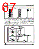
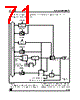
67 / 184 page  ST10F269 12 - PARALLEL PORTS 67/184 Figure 23 : PORT1 I/O and Alternate Functions When an external bus mode is enabled, the direction of the port pin and the loading of data into the port output latch are controlled by the bus controller hardware. The input of the port Buffer latch is disconnected from the internal bus and is switched to the line labeled “Alternate Data Output” via a multiplexer. The alternate data is the 16-bit intra-segment address. While an external bus mode is enabled, the user software should not write to the port output latch, otherwise unpredictable results may occur. When the external bus modes are disabled, the contents of the direction register last written by the user becomes active. The Figure 24 shows the structure of a PORT1 pin. PORT1 P1H P1L Alternate Function a) General Purpose Input/Output 8/16-bit Demultiplexed Bus b) CAPCOM2 Capture Inputs only P1H.7 P1H.6 P1H.5 P1H.4 P1H.3 P1H.2 P1H.1 P1H.0 P1L.7 P1L.6 P1L.5 P1L.4 P1L.3 P1L.2 P1L.1 P1L.0 A15 A14 A13 A12 A11 A10 A9 A8 A7 A6 A5 A4 A3 A2 A1 A0 CC27IO CC26IO CC25IO CC24IO Figure 24 : Block Diagram of a PORT1 Pin Direction Latch Write DP1H.y / DP1L.y Read DP1H.y / DP1L.y Port Output Latch Write P1H.y / P1L.y Read P1H.y / P1L.y MUX 0 1 MUX 0 1 MUX 0 1 “1” Input Latch Clock P1H.y P1L.y Output Buffer y = 7...0 Alternate Function Enable Port Data Output Alternate Data Output |
|
Lien URL |
| ALLDATASHEET vous a-t-il été utile ? [ DONATE ] |
À propos de Alldatasheet | Publicité | Contactez-nous | Politique de confidentialité | Lien vers la fiche technique | Echange de liens | Fabricants All Rights Reserved©Alldatasheet.com |
| Russian : Alldatasheetru.com | Korean : Alldatasheet.co.kr | Spanish : Alldatasheet.es | French : Alldatasheet.fr | Italian : Alldatasheetit.com Portuguese : Alldatasheetpt.com | Polish : Alldatasheet.pl | Vietnamese : Alldatasheet.vn Indian : Alldatasheet.in | Mexican : Alldatasheet.com.mx | British : Alldatasheet.co.uk | New Zealand : Alldatasheet.co.nz |
|
Family Site : ic2ic.com |
icmetro.com |
 French ▼
 English
 Chinese
 German
 Japanese
 Russian
 Korean
 Spanish
 French
 Italian
 Portuguese
 Polish
 Vietnamese
 Indian
 Mexican
 British
 New Zealand