|
Moteur de recherche de fiches techniques de composants électroniques |
|
|
Moteur de recherche de fiches techniques de composants électroniques |
|
ST10F269Z1Q6 Fiches technique(PDF) 16 Page - STMicroelectronics |
|
|
|||||||||||||||||||||||||||||
ST10F269Z1Q6 Fiches technique(HTML) 16 Page - STMicroelectronics |
|
|
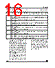
16 / 184 page  4 - MEMORY ORGANIZATION ST10F269 16/184 XPERCON (F024h / 12h) ESFR Reset Value: - - 05h Note: - When both CAN are disabled via XPER- CON setting, then any access in the address range 00’EE00h - 00’EFFFh will be directed to external memory interface, using the BUSCONx register correspond- ing to address matching ADDRSELx regis- ter. P4.4 and P4.7 can be used as General Purpose I/O when CAN2 is disabled, and P4.5 and P4.6 can be used as General Purpose I/O when CAN1 is disabled. - The default XPER selection after Reset is identical to XBUS configuration of ST10C167: XCAN1 is enabled, XCAN2 is disabled, XRAM1 (2K Byte compatible XRAM) is enabled, XRAM2 (new 8K Byte XRAM) is disabled. - Register XPERCON cannot be changed after the global enabling of XPeripherals, i.e. after the setting of bit XPEN in the SYSCON register. - In EMUlation mode, all the XPERipherals are enabled (XPERCON bit are all set). The access to external memory and/or XBus is controlled by the bondout chip. - When the Real Time Clock is disabled (RTCEN = 0), the clock oscillator is switch-off if the ST10 enters in power-down mode. Otherwise, when the Real Time Clock is enabled, the bit RTCOFF of the RTCCON register allows to choose the power-down mode of the clock oscillator (See Chapter : Real Time Clock on page 105). 15 14 13 12 11 10 9 8 7 6 5 4 3 2 1 0 - - --- --- - -- RTCEN XRAM2EN XRAM1EN CAN2EN CAN1EN RW RW RW RW RW CAN1EN CAN1 Enable Bit ‘0’: Accesses to the on-chip CAN1 XPeripheral and its functions are disabled. P4.5 and P4.6 pins can be used as general purpose I/Os. Address range 00’EF00h-00’EFFFh is only directed to external memory if CAN2EN is also ‘0’. ‘1’: The on-chip CAN1 XPeripheral is enabled and can be accessed. CAN2EN CAN2 Enable Bit ‘0’: Accesses to the on-chip CAN2 XPeripheral and its functions are disabled. P4.4 and P4.7 pins can be used as general purpose I/Os. Address range 00’EE00h-00’EEFFh is only directed to external memory if CAN1EN is also ‘0’. ‘1’: The on-chip CAN2 XPeripheral is enabled and can be accessed. XRAM1EN XRAM1 Enable Bit ‘0’: Accesses to external memory within space 00’E000h to 00’E7FFh. The 2K Bytes of internal XRAM1 are disabled. ’1’: Accesses to the internal 2K Bytes of XRAM1. XRAM2EN XRAM2 Enable Bit ‘0’: Accesses to the external memory within space 00’C000h to 00’DFFFh. The 8K Bytes of internal XRAM2 are disabled. ’1’: Accesses to the internal 8K Bytes of XRAM2. RTCEN RTC Enable Bit ’0’: Accesses to the on-chip Real Time Clock are disabled, external access is performed. Address range 00’EC00h-00’ECFFh is only directed to external memory if CAN1EN and CAN2EN are ’0’ also ’1’: The on-chip Real Time Clock is enabled and can be accessed. |
|
Lien URL |
| ALLDATASHEET vous a-t-il été utile ? [ DONATE ] |
À propos de Alldatasheet | Publicité | Contactez-nous | Politique de confidentialité | Lien vers la fiche technique | Echange de liens | Fabricants All Rights Reserved©Alldatasheet.com |
| Russian : Alldatasheetru.com | Korean : Alldatasheet.co.kr | Spanish : Alldatasheet.es | French : Alldatasheet.fr | Italian : Alldatasheetit.com Portuguese : Alldatasheetpt.com | Polish : Alldatasheet.pl | Vietnamese : Alldatasheet.vn Indian : Alldatasheet.in | Mexican : Alldatasheet.com.mx | British : Alldatasheet.co.uk | New Zealand : Alldatasheet.co.nz |
|
Family Site : ic2ic.com |
icmetro.com |
 French ▼
 English
 Chinese
 German
 Japanese
 Russian
 Korean
 Spanish
 French
 Italian
 Portuguese
 Polish
 Vietnamese
 Indian
 Mexican
 British
 New Zealand