|
Moteur de recherche de fiches techniques de composants électroniques |
|
|
Moteur de recherche de fiches techniques de composants électroniques |
|
5M40ZE64C5N Fiches technique(PDF) 12 Page - Altera Corporation |
|
|
|||||||||||||||||||||||||||||
5M40ZE64C5N Fiches technique(HTML) 12 Page - Altera Corporation |
|
|
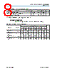
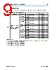
12 / 30 page  3–12 Chapter 3: DC and Switching Characteristics for MAX V Devices Timing Model and Specifications MAX V Device Handbook May 2011 Altera Corporation Internal Timing Parameters Internal timing parameters are specified on a speed grade basis independent of device density. Table 3–18 through Table 3–25 on page 3–19 list the MAX V device internal timing microparameters for LEs, input/output elements (IOEs), UFM blocks, and MultiTrack interconnects. f For more information about each internal timing microparameters symbol, refer to AN629: Understanding Timing in Altera CPLDs. UFM 512 × 16 None 3 1 10.0 10.0 10.0 10.0 MHz 512 × 16 SPI (2) 37 1 9.7 9.7 8.0 8.0 MHz 512 × 8 Parallel (3) 73 1 (4) (4) (4) (4) MHz 512 × 16 I2C (3) 142 1 100 (5) 100 (5) 100 (5) 100 (5) kHz Notes to Table 3–17: (1) This design is a binary loadable up counter. (2) This design is configured for read-only operation in Extended mode. Read and write ability increases the number of logic elements (LEs) used. (3) This design is configured for read-only operation. Read and write ability increases the number of LEs used. (4) This design is asynchronous. (5) The I2C megafunction is verified in hardware up to 100-kHz serial clock line rate. Table 3–17. Device Performance for MAX V Devices (Part 2 of 2) Resource Used Design Size and Function Resources Used Performance Unit 5M40Z/ 5M80Z/ 5M160Z/ 5M240Z/ 5M570Z 5M1270Z/ 5M2210Z Mode LEs UFM Blocks C4 C5, I5 C4 C5, I5 Table 3–18. LE Internal Timing Microparameters for MAX V Devices (Part 1 of 2) Symbol Parameter 5M40Z/ 5M80Z/ 5M160Z/ 5M240Z/ 5M570Z 5M1270Z/ 5M2210Z Unit C4 C5, I5 C4 C5, I5 Min Max Min Max Min Max Min Max tLUT LE combinational look-up table (LUT) delay — 1,215 — 2,247 — 742 — 914 ps tCOMB Combinational path delay — 243 — 309 — 192 — 236 ps tCLR LE register clear delay 401 — 545 — 309 — 381 — ps tPRE LE register preset delay 401 — 545 — 309 — 381 — ps tSU LE register setup time before clock 260 — 321 — 271 — 333 — ps tH LE register hold time after clock 0 —0 —0 —0 — ps tCO LE register clock-to-output delay — 380 — 494 — 305 — 376 ps |
|
Lien URL |
| ALLDATASHEET vous a-t-il été utile ? [ DONATE ] |
À propos de Alldatasheet | Publicité | Contactez-nous | Politique de confidentialité | Lien vers la fiche technique | Echange de liens | Fabricants All Rights Reserved©Alldatasheet.com |
| Russian : Alldatasheetru.com | Korean : Alldatasheet.co.kr | Spanish : Alldatasheet.es | French : Alldatasheet.fr | Italian : Alldatasheetit.com Portuguese : Alldatasheetpt.com | Polish : Alldatasheet.pl | Vietnamese : Alldatasheet.vn Indian : Alldatasheet.in | Mexican : Alldatasheet.com.mx | British : Alldatasheet.co.uk | New Zealand : Alldatasheet.co.nz |
|
Family Site : ic2ic.com |
icmetro.com |
 French ▼
 English
 Chinese
 German
 Japanese
 Russian
 Korean
 Spanish
 French
 Italian
 Portuguese
 Polish
 Vietnamese
 Indian
 Mexican
 British
 New Zealand