|
Moteur de recherche de fiches techniques de composants électroniques |
|
|
Moteur de recherche de fiches techniques de composants électroniques |
|
ADIS16240ABCZ Fiches technique(PDF) 15 Page - Analog Devices |
|
|
|||||||||||||||||||||||||||||
ADIS16240ABCZ Fiches technique(HTML) 15 Page - Analog Devices |
|
|
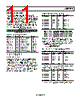
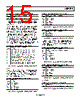
15 / 16 page  ADIS16240 Rev. 0 | Page 15 of 16 Table 27. XACCL_OFF, YACCL_OFF, ZACCL_OFF1 Bit Description (Default = 0x0000) [15:10] Unused [9:0] Offset, twos complement, 51.4 mg/LSB 1 The XACCL_OFF register is located at Address 0x21[15:8] and Address 0x20[7:0]. The YACCL_OFF register is located at Address 0x23[15:8] and Address 0x22[7:0]. The ZACCL_OFF register is located at Address 0x25[15:8] and Address 0x24[7:0]. Diagnostics For all of the error flags in the DIAG_STAT register (see Table 28), a 1 identifies an error condition, and a 0 signals normal operation. All of the flags return to 0 after reading DIAG_STAT. If the power supply is still out of range during the next sample cycle, DIAG_ STAT[0] and DIAG_STAT[1] return to 1. DIAG_STAT[9:8] pro- vide flags to check for the alarms with respect to the conditions in the ALM_CTRL and ALM_MAGx registers. DIAG_STAT[6] contains the internal memory checksum result. If the sum of the firmware program memory does not does not match the expected value, this flag reports a 1. The SPI communication flag (DIAG_ STAT[3]) changes to 1 when the number of SCLK pulses during a SPI transfer is not a multiple of 16 when CS goes high. Table 28. DIAG_STAT Register Bit Descriptions1 Bit Description (Default = 0x0000) [15:10] Unused 9 Alarm 2 status: 1 = alarm active, 0 = alarm inactive 8 Alarm 1 status: 1 = alarm active, 0 = alarm inactive 7 Capture buffer full: 1 = capture buffer is full 6 Flash test, checksum flag: 1 = mismatch, 0 = match 5 Power-on, self-test flag: 1 = failure, 0 = pass 4 Power-on self-test: 1 = in-progress, 0 = complete 3 SPI communications failure: 1 = error, 0 = normal 2 Flash update failure: 1 = failure, 0 = pass 1 Power supply above 3.625 V: 1 = above, 0 = below 0 Power supply below 2.225 V: 1 = below, 0 = above 1 The DIAG_STAT register is located at Address 0x1B[15:8] and Address 0x1A[7:0]. Clock The CLK_TIME, CLK_DATE, and CLK_YEAR registers provide an internal clock that enables a time entry into the event header and for user access. If CLK_TIME = 0x2231, the time is 22:31, or 10:31 p.m. The CLK_DATE and CLK_YEAR registers follow a similar binary-coded, decimal format. Table 29. CLK_TIME Register Bit Descriptions1 Bit Description [15:14] Unused [13:12] Hours, 10s digit [11:8] Hours, 1s digit 7 Unused [6:4] Minutes, 10s digit [3:0] Minutes, 1s digit 1 The CLK_TIME register is located at Address 0x2F[15:8] and Address 0x2E[7:0]. Table 30. CLK_DATE Register Bit Descriptions1 Bit Description (Default = 0x0000) [15:13] Unused 12 Month, 10s digit [11:8] Month, 1s digit [7:6] Unused [5:4] Day, 10s digit [3:0] Day, 1s digit 1 The CLK_DATE register is located at Address 0x31[15:8] and Address 0x30[7:0]. Table 31. CLK_YEAR Register Bit Descriptions1 Bit Description (Default = 0x0000) [15:8] Unused [7:4] Year, 10s digit [3:0] Year, 1s digit 1 The CLK_YEAR register is located at Address 0x33[15:8] and Address 0x32[7:0]. The WAKE_TIME and WAKE_DATE registers enable users to program a specific time for the ADIS16240 to exit standby mode. Enable this function by writing the wake-up time and date to these registers. Table 32. WAKE_TIME Register Bit Descriptions1 Bit Description (Default = 0x0000) 15 Wake time enable (1 = enabled, 0 = disabled) 14 Unused [13:12] Hours, 10s digit [11:8] Hours, 1s digit 7 Unused [6:4] Minutes, 10s digit [3:0] Minutes, 1s digit 1 The WAKE_TIME register is located at Address 0x35[15:8] and Address 0x34[7:0]. Table 33. WAKE_DATE Register Bit Descriptions1 Bit Description (Default = 0x0000) [15:14] Unused [13:12] Month, 10s digit [11:8] Month, 1s digit [7:6] Unused [5:4] Day, 10s digit [3:0] Day, 1s digit 1 The WAKE_DATE register is located at Address 0x37[15:8] and Address 0x36[7:0]. Checksum Table 34. CHK_SUM Register Bit Descriptions1 Bit Description [15:0] Sum of memory locations used to verify code integrity 1 The CHK_SUM register is located at Address 0x1F[15:8] and Address 0x1E[7:0]. |
|
|
Lien URL |
| ALLDATASHEET vous a-t-il été utile ? [ DONATE ] |
À propos de Alldatasheet | Publicité | Contactez-nous | Politique de confidentialité | Lien vers la fiche technique | Echange de liens | Fabricants All Rights Reserved©Alldatasheet.com |
| Russian : Alldatasheetru.com | Korean : Alldatasheet.co.kr | Spanish : Alldatasheet.es | French : Alldatasheet.fr | Italian : Alldatasheetit.com Portuguese : Alldatasheetpt.com | Polish : Alldatasheet.pl | Vietnamese : Alldatasheet.vn Indian : Alldatasheet.in | Mexican : Alldatasheet.com.mx | British : Alldatasheet.co.uk | New Zealand : Alldatasheet.co.nz |
|
Family Site : ic2ic.com |
icmetro.com |
 French ▼
 English
 Chinese
 German
 Japanese
 Russian
 Korean
 Spanish
 French
 Italian
 Portuguese
 Polish
 Vietnamese
 Indian
 Mexican
 British
 New Zealand