|
Moteur de recherche de fiches techniques de composants électroniques |
|
|
Moteur de recherche de fiches techniques de composants électroniques |
|
ADIS16240ABCZ Fiches technique(PDF) 11 Page - Analog Devices |
|
|
|||||||||||||||||||||||||||||
ADIS16240ABCZ Fiches technique(HTML) 11 Page - Analog Devices |
|
|
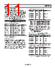
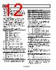
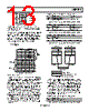
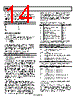
11 / 16 page  ADIS16240 Rev. 0 | Page 11 of 1 6 OUTPUT DATA REGISTERS Each output data register uses the bit assignments shown in Figure 19. The ND flag indicates that unread data resides in the register. This flag clears and returns to 0 after reading the register. It returns to 1 after the next internal sample updates the register with new data. When the data-ready function (the DIO1 and DIO2 pins and the MSC_CTRL register; see Table 25) drives data collection, the ND bit is always high and does not require validation. The EA flag indicates that one of the error flags in the DIAG_STAT register (see Table 28) is active (true). MSB FOR 10-BIT OUTPUT ND EA x x x x D9D8D7D6D5D4 D3D2D1 D0 Figure 19. Output Register Bit Assignments Table 8. Output Data Register Formats Register Bits Format Scale SUPPLY_OUT 10 Binary, 0 V = 0x0000 4.88 mV XACCL_OUT 10 Twos complement 51.4 mg YACCL_OUT 10 Twos complement 51.4 mg ZACCL_OUT 10 Twos complement 51.4 mg AUX_ADC 10 Binary, 0 V = 0x0000 VDD/1024 TEMP_OUT 10 Binary, 25°C = 0x0133 0.244°C XPEAK_OUT1 10 Twos complement 51.4 mg YPEAK_OUT1 10 Twos complement 51.4 mg ZPEAK_OUT1 10 Twos complement 51.4 mg XYZPEAK_OUT2 12 Binary, 0 g2 = 0x0000 0.676 g2 1 Function requires MSC_CTRL[14] = 1. 2 Function requires MSC_CTRL[15] = 1. Processing Sensor Data Processing sensor data starts with reading the appropriate output data register using the SPI. For example, use DIN = 0x0E00 to read the XPEAK_OUT register. Use the ND and EA bits to validate new data and normal operating status, if necessary. Then mask off all of the nondata bits and calculate the data, using the format and scale information shown in Table 8. For example, XACCL_OUT[9:0] and XYZPEAK_OUT[11:0] contain all relevant data for their function. Table 9, Table 10, and Table 11 provide output code examples for each output register. Table 9. Accelerometer Data Output Format1 Binary Hex Codes Acceleration 01 0011 0111 0x137 +311 +16 g … … … … 00 0000 0010 0x002 +2 +102.8 mg 00 0000 0001 0x001 +1 +51.4 mg 00 0000 0000 0x000 0 0 11 1111 1111 0x3FF −1 −51.4 mg 11 1111 1110 0x3FE −2 −102.8 mg … … … … 10 1100 1001 0x2C9 −311 −16 g 1 The XACCL_OUT register is located at Address 0x05[15:8] and Address 0x04[7:0]. The YACCL_OUT register is located at Address 0x07[15:8] and Address 0x06[7:0]. The ZACCL_OUT register is located at Address 0x09[15:8] and Address 0x08[7:0]. The XPEAK_OUT register is located at Address 0x0F[15:8] and Address 0x0E[7:0]. The YPEAK_OUT register is located at Address 0x11[15:8] and Address 0x10[7:0]. The ZPEAK_OUT register is located at Address 0x13[15:8] and Address 0x12[7:0]. When MSC_CTRL[14] = 1, the XPEAK_OUT, YPEAK_OUT, and ZPEAK_OUT registers track the peak acceleration in each acceleration output register. When MSC_CTRL[15] = 1, use the following equation to calculate the root mean square (rms) of all three peak registers, where 1 LSB = 0.822 g: OUT XYZPEAK XYZ rms _ = Set GLOB_CMD[5] = 1 to reset these registers to 0x0000. Table 10. Power Supply Data Output Format1 Binary Hex Codes Power Supply (V) 10 1110 0010 0x2E2 738 3.6 … … … … 10 1010 0101 0x2A5 677 3.30488 10 1010 0100 0x2A4 676 3.3 10 1010 0011 0x2A3 675 3.29502 … … … … 01 1110 1100 0x1EC 492 2.4 1 The SUPPLY_OUT register is located at Address 0x03[15:8] and Address 0x02[7:0]. Table 11. Temperature Data Output Format1 Binary Hex Codes Temperature (°C) 10 0010 1001 0x229 553 +85°C … … … … 01 0011 0100 0x134 308 +25.244°C 01 0011 0011 0x133 307 +25°C 01 0011 0010 0x132 306 +24.756°C … … … … 00 0010 1001 0x029 41 −40°C 1 The TEMP_OUT register is located at Address 0x0D[15:8] and Address 0x0C[7:0]. |
|
|
Lien URL |
| ALLDATASHEET vous a-t-il été utile ? [ DONATE ] |
À propos de Alldatasheet | Publicité | Contactez-nous | Politique de confidentialité | Lien vers la fiche technique | Echange de liens | Fabricants All Rights Reserved©Alldatasheet.com |
| Russian : Alldatasheetru.com | Korean : Alldatasheet.co.kr | Spanish : Alldatasheet.es | French : Alldatasheet.fr | Italian : Alldatasheetit.com Portuguese : Alldatasheetpt.com | Polish : Alldatasheet.pl | Vietnamese : Alldatasheet.vn Indian : Alldatasheet.in | Mexican : Alldatasheet.com.mx | British : Alldatasheet.co.uk | New Zealand : Alldatasheet.co.nz |
|
Family Site : ic2ic.com |
icmetro.com |
 French ▼
 English
 Chinese
 German
 Japanese
 Russian
 Korean
 Spanish
 French
 Italian
 Portuguese
 Polish
 Vietnamese
 Indian
 Mexican
 British
 New Zealand