|
Moteur de recherche de fiches techniques de composants électroniques |
|
|
Moteur de recherche de fiches techniques de composants électroniques |
|
ADIS16240ABCZ Fiches technique(PDF) 14 Page - Analog Devices |
|
|
|||||||||||||||||||||||||||||
ADIS16240ABCZ Fiches technique(HTML) 14 Page - Analog Devices |
|
|
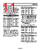
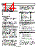
14 / 16 page  ADIS16240 Rev. 0 | Page 14 of 1 6 Transient Behavior During Capture During capture events, the device consumes an increased amount of current for a short period. Following a capture event, sampling suspends and the SPI commands are ignored by the sensor for the pause times that are listed in Table 22. Table 22. Postcapture Operation Pause Times Event Length (Samples) Pause Time (ms) <64 2 128 4 256 8 512 16 1024 33 OPERATIONAL CONTROL Internal Sample Rate The SMPL_PRD register (see Table 23) provides a user control for sample rate adjustment, using the following equation: fS = ) 1 ( 32768 + SR N For example, set SMPL_PRD[7:0] = 0x07 (DIN = 0xC807) to configure the ADIS16240 to operate at its maximum sample rate of 4096 SPS. Note that the sample rate affects power dis- sipation and peak resolution during event capture. Table 23. SMPL_PRD Register Bit Descriptions1 Bit Description (Default = 0x001F) [15:0] Sample rate scale factor, binary format (NSR) 1 The SMPL_PRD register is located at Address 0x49[15:8] and Address 0x48[7:0]. Global Commands For convenience, the GLOB_CMD register (see Table 24) provides an array of single-write commands. Setting the assigned bit to 1 activates each function, right after the 16th SCLK in the SPI com- munication sequence. When the function completes, the bit restores itself to 0. All commands in the GLOB_CMD register require the power supply to be within normal limits for the execution times listed in Table 24. The execution times reflect the factory default configuration, where applicable, and describe the time required to return to normal operation. For example, set GLOB_CMD[2] = 1 (DIN = 0xCA04) to place the part in standby mode. Set GLOB_CMD[8] = 1 (DIN = 0xCB01) to wake up the device and return to normal operation. Input/Output Lines The ADIS16240 provides two general-purpose digital input/ output lines that offer several functions. When using the factory- default configuration, MSC_CTRL[2:0] establishes DIO1 as a positive data-ready output. Change MSC_CTRL[2:0] to 100 (DIN = 0xC604) to make DIO1 a negative data-ready output signal. ALM_CTRL[2:0] offers a control for setting one of the digital signals as an alarm indicator. For example, set ALM_ CTRL[2:0] = 110 (DIN = 0xBC06) to set DIO1 as a positive alarm indicator output signal. When configured as general- purpose lines, the GPIO_CTRL register configures DIO1 and DIO2. For example, set GPIO_CTRL = 0x0103 (DIN = 0xC403, then 0xC501) to set DIO1 and DIO2 as outputs, with DIO1 in a 1 state and DIO2 in a 0 state. In the event of competing assign- ments, the order of precedence is MSC_CTRL, ALM_CTRL, and GPIO_CTRL. Table 24. GLOB_CMD Register Bit Descriptions1 Bit Description Execution Time2 [15:9] Unused N/A 8 Wake up from standby mode 0.2 ms 7 Software reset 32 ms 6 Clear capture buffer flash memory 350 ms 5 Clear peak registers N/A 4 Clear DIAG_STAT register N/A 3 Save configuration to flash 24 ms 2 Start standby mode for low power N/A 1 Restore factory-default settings 350 ms 0 Auto-null N/A 1 The GLOB_CMD register is located at Address 0x4B[15:8] and Address 0x4A[7:0]. 2 SPI processing and data sampling suspend for the indicated times. Table 25. MSC_CTRL Register Bit Descriptions1 Bit Description (Default = 0x0006) 15 Enables sum-of-squares output (XYZPEAK_OUT) 14 Enables peak tracking output (XPEAK_OUT, YPEAK_OUT, and ZPEAK_OUT) [13:10] Unused 9 No self-test on startup when set to 1 8 Self-test enable: 1 = apply electrostatic force, 0 = disabled [7:3] Unused 2 Data-ready enable: 1 = enabled, 0 = disabled 1 Data-ready polarity: 1 = active high, 0 = active low 0 Data-ready line selection: 1 = DIO2, 0 = DIO1 1 The MSC_CTRL register is located at Address 0x47[15:8] and Address 0x46[7:0]. Table 26. GPIO_CTRL Register Bit Descriptions1 Bit Description (Default = 0x0000) [15:10] Unused 9 General-Purpose I/O Line 2 data level 8 General-Purpose I/O Line 1 data level [7:2] Unused 1 General-Purpose I/O Line 2, data direction control: 1 = output, 0 = input 0 General-Purpose I/O Line 1, data direction control: 1 = output, 0 = input 1 The GPIO_CTRL register is located at Address 0x45[15:8] and Address 0x44[7:0]. Offset Adjustment The XACCL_OUT, YACCL_OFF, and ZACCL_OFF registers add to the sensor outputs and provide a convenient offset adjust- ment function for each accelerometer output. For example, writing 0x0A to YACCL_OUT[7:0] (DIN = 0xA20A) results in a 514 mg offset adjustment for the YACCL_OUT output data. |
|
|
Lien URL |
| ALLDATASHEET vous a-t-il été utile ? [ DONATE ] |
À propos de Alldatasheet | Publicité | Contactez-nous | Politique de confidentialité | Lien vers la fiche technique | Echange de liens | Fabricants All Rights Reserved©Alldatasheet.com |
| Russian : Alldatasheetru.com | Korean : Alldatasheet.co.kr | Spanish : Alldatasheet.es | French : Alldatasheet.fr | Italian : Alldatasheetit.com Portuguese : Alldatasheetpt.com | Polish : Alldatasheet.pl | Vietnamese : Alldatasheet.vn Indian : Alldatasheet.in | Mexican : Alldatasheet.com.mx | British : Alldatasheet.co.uk | New Zealand : Alldatasheet.co.nz |
|
Family Site : ic2ic.com |
icmetro.com |
 French ▼
 English
 Chinese
 German
 Japanese
 Russian
 Korean
 Spanish
 French
 Italian
 Portuguese
 Polish
 Vietnamese
 Indian
 Mexican
 British
 New Zealand