|
Moteur de recherche de fiches techniques de composants électroniques |
|
|
Moteur de recherche de fiches techniques de composants électroniques |
|
ADIS16240ABCZ Fiches technique(PDF) 9 Page - Analog Devices |
|
|
|||||||||||||||||||||||||||||
ADIS16240ABCZ Fiches technique(HTML) 9 Page - Analog Devices |
|
|
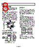
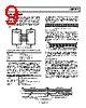
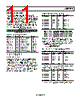
9 / 16 page  ADIS16240 Rev. 0 | Page 9 of 16 BASIC OPERATION The ADIS16240 starts up automatically when it has a valid power supply and begins producing digital acceleration data in the output registers. When using the factory-default configuration, DIO1 serves as a data-ready indicator signal that can drive a processor interrupt function. Figure 14 shows a schematic for connecting to a SPI-compatible processor platform, referred to as the SPI master. CS ADIS16240 SPI SLAVE SCLK DIN DOUT DIO1 DIO2 SS VDD VDD SYSTEM PROCESSOR SPI MASTER SCLK MOSI MISO IRQ1 IRQ2 Figure 14. Electrical Hook-Up Diagram Table 5. Generic Master Processor Pin Names and Functions Pin Name Function SS Slave select. IRQ1, IRQ2 Interrupt request inputs. MOSI Master output, slave input. MISO Master input, slave output. SCLK Serial clock. The ADIS16240 SPI interface supports full duplex serial commu- nication (simultaneous transmit and receive) and uses the bit sequence shown in Figure 18. Processor platforms typically support SPI communication with general-purpose serial ports that require some configuration in their control registers. Table 6 lists the most common settings that require attention when initializing a pro- cessor serial port for communication with the ADIS16240. Table 6. Generic Master Processor SPI Settings Processor Setting Description Master The ADIS16240 operates as a slave. SCLK Rate ≤ 2.5 MHz Bit rate setting. SPI Mode 3 (1,1) Clock polarity/phase (CPOL = 1, CPHA = 1). MSB First Bit sequence. 16-Bit Shift register/data length. User registers govern all data collection and configuration. Table 7 provides a memory map that includes all user registers, along with references to bit assignment tables that follow the generic assign- ments in Figure 15. UPPER BYTE 15 14 13 12 11 10 9 8 7 6 5 4 3 2 1 0 LOWER BYTE Figure 15. Generic Register Bit Assignments SPI Write Commands Master processors write to the control registers, one byte at a time, using the bit assignments shown in Figure 18. The program- mable registers in Table 7 provide controls for optimizing sensor operation and for starting various automated functions. For example, set GLOB_CMD[8] = 1 (DIN = 0xCB01) to wake up the device. CS DIN SCLK Figure 16. SPI Sequence for a Wake-Up Command (DIN = 0xCB01) Some configurations require writing both bytes to a register, which takes two separate 16-bit sequences. See GLOB_CMD[3] in Table 24 for backing up configuration data in nonvolatile flash memory. SPI Read Commands Reading data on the SPI requires two consecutive 16-bit sequences. The first sequence transmits the read command on DIN, and the second sequence receives the resulting data from DOUT. The 7-bit register address can represent either the upper or lower byte address for the target register. For example, DIN can be either 0x0200 or 0x0300 when reading the SUPPLY_OUT register. The SPI operates in full duplex mode, which means that the master processor can read the output data from DOUT while using the same SCLK pulses to transmit a new command on DIN. In Figure 17, the second SPI segment sets up the device to read YACCL_OUT on the following SPI segment (not shown). CS DIN SCLK DIN = 0x0400 PRODUCES XACCL_OUT CONTENTS ON DOUT DURING THE NEXT SPI SEGMENT DOUT SPI SEGMENT 1 SPI SEGMENT 2 DOUT = 0x802B = 2.21g, NEW DATA DIN = 0x0600 TO READ YACCL_OUT Figure 17. Example SPI Read Sequence |
|
|
Lien URL |
| ALLDATASHEET vous a-t-il été utile ? [ DONATE ] |
À propos de Alldatasheet | Publicité | Contactez-nous | Politique de confidentialité | Lien vers la fiche technique | Echange de liens | Fabricants All Rights Reserved©Alldatasheet.com |
| Russian : Alldatasheetru.com | Korean : Alldatasheet.co.kr | Spanish : Alldatasheet.es | French : Alldatasheet.fr | Italian : Alldatasheetit.com Portuguese : Alldatasheetpt.com | Polish : Alldatasheet.pl | Vietnamese : Alldatasheet.vn Indian : Alldatasheet.in | Mexican : Alldatasheet.com.mx | British : Alldatasheet.co.uk | New Zealand : Alldatasheet.co.nz |
|
Family Site : ic2ic.com |
icmetro.com |
 French ▼
 English
 Chinese
 German
 Japanese
 Russian
 Korean
 Spanish
 French
 Italian
 Portuguese
 Polish
 Vietnamese
 Indian
 Mexican
 British
 New Zealand