|
Moteur de recherche de fiches techniques de composants électroniques |
|
|
Moteur de recherche de fiches techniques de composants électroniques |
|
APX9292 Fiches technique(PDF) 6 Page - Anpec Electronics Coropration |
|
|
|||||||||||||||||||||||||||||
APX9292 Fiches technique(HTML) 6 Page - Anpec Electronics Coropration |
|
|
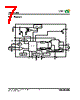
6 / 18 page  Copyright © ANPEC Electronics Corp. Rev. A.3 - Apr., 2017 www.anpec.com.tw 6 APX9292 PIN NO. NAME FUNCTION 1 OUT2 H-bridge Output Connection. 2 VCC Supply Voltage Input Pin. 3 MIN Minimum Speed Setting. An external voltage into MIN pin to set fan speed. 4 SET Speed Setting. An external voltage into SET pin to set fan speed. 5 OSC Oscillation Frequency Setting. Connect a capacitor to GND to set oscillation frequency. 6 FG Rotation Speed Output. This is an open –drain output. 7 NC No Connection. 8 IN+ Hall Input +. Connect to hall element positive output. 9 HB Hall Bias. This is a 1.3V constant –voltage output for hall element bias. 10 IN- Hall Input -. Connect to hall element negative output. 11 6VREG 6V Regulator Output. This is a 6V constant-voltage output for application circuit biases. 12 CT Shutdown Time and Restart Time Setting. Connect a capacitor to GND to set shutdown time and restart time in lock mode. 13 SGND Control Stage GND. 14 OUT1 H-bridge Output Connection. Pin Descriptions Note : PGND pads are power ground of driver circuit. Please connect to input power. |
|
|
Lien URL |
| ALLDATASHEET vous a-t-il été utile ? [ DONATE ] |
À propos de Alldatasheet | Publicité | Contactez-nous | Politique de confidentialité | Lien vers la fiche technique | Echange de liens | Fabricants All Rights Reserved©Alldatasheet.com |
| Russian : Alldatasheetru.com | Korean : Alldatasheet.co.kr | Spanish : Alldatasheet.es | French : Alldatasheet.fr | Italian : Alldatasheetit.com Portuguese : Alldatasheetpt.com | Polish : Alldatasheet.pl | Vietnamese : Alldatasheet.vn Indian : Alldatasheet.in | Mexican : Alldatasheet.com.mx | British : Alldatasheet.co.uk | New Zealand : Alldatasheet.co.nz |
|
Family Site : ic2ic.com |
icmetro.com |
 French ▼
 English
 Chinese
 German
 Japanese
 Russian
 Korean
 Spanish
 French
 Italian
 Portuguese
 Polish
 Vietnamese
 Indian
 Mexican
 British
 New Zealand