|
Moteur de recherche de fiches techniques de composants électroniques |
|
|
Moteur de recherche de fiches techniques de composants électroniques |
|
AK8975 Fiches technique(PDF) 20 Page - Asahi Kasei Microsystems |
|
|
|||||||||||||||||||||||||||||
AK8975 Fiches technique(HTML) 20 Page - Asahi Kasei Microsystems |
|
|
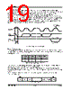
20 / 34 page  [AK8975/C] 7.2.2. WRITE Instruction When the R/W bit is set to "0", AK8975/C performs write operation. In write operation, AK8975/C generates an acknowledge after receiving a start condition and the first byte (slave address) then receives the second byte. The second byte is used to specify the address of an internal control register and is based on the MSB-first configuration. MSB LSB A7 A6 A5 A4 A3 A2 A1 A0 Figure 7.7 Register Address After receiving the second byte (register address), AK8975/C generates an acknowledge then receives the third byte. The third and the following bytes represent control data. Control data consists of 8 bits and is based on the MSB-first configuration. AK8975/C generates an acknowledge after every byte is received. Data transfer always stops with a stop condition generated by the master. MSB LSB D7 D6 D5 D4 D3 D2 D1 D0 Figure 7.8 Control Data AK8975/C can write multiple bytes of data at a time. After reception of the third byte (control data), AK8975/C generates an acknowledge then receives the next data. If additional data is received instead of a stop condition after receiving one byte of data, the address counter inside the LSI chip is automatically incremented and the data is written at the next address. The address is incremented from 00H to 0CH or from 10H to12H. When the address is in the range from 00H to 0CH, the address goes back to 00H after 0CH. When the address is in the range from 10H to 12H, the address goes back to 10H after 12H. Actual data is written only to Read/Write registers (0AH to 0FH). SDA S T A R T A C K A C K S Slave Address A C K Register Address(n) Data(n) P S T O P Data(n+x) A C K Data(n+1) A C K A C K R/W= "0" Figure 7.9 WRITE Instruction MS1187-E-02 - 20 - 2010/05 |
|
Lien URL |
| ALLDATASHEET vous a-t-il été utile ? [ DONATE ] |
À propos de Alldatasheet | Publicité | Contactez-nous | Politique de confidentialité | Lien vers la fiche technique | Echange de liens | Fabricants All Rights Reserved©Alldatasheet.com |
| Russian : Alldatasheetru.com | Korean : Alldatasheet.co.kr | Spanish : Alldatasheet.es | French : Alldatasheet.fr | Italian : Alldatasheetit.com Portuguese : Alldatasheetpt.com | Polish : Alldatasheet.pl | Vietnamese : Alldatasheet.vn Indian : Alldatasheet.in | Mexican : Alldatasheet.com.mx | British : Alldatasheet.co.uk | New Zealand : Alldatasheet.co.nz |
|
Family Site : ic2ic.com |
icmetro.com |
 French ▼
 English
 Chinese
 German
 Japanese
 Russian
 Korean
 Spanish
 French
 Italian
 Portuguese
 Polish
 Vietnamese
 Indian
 Mexican
 British
 New Zealand