|
Moteur de recherche de fiches techniques de composants électroniques |
|
|
Moteur de recherche de fiches techniques de composants électroniques |
|
ST10F269Z1Q3 Fiches technique(PDF) 50 Page - STMicroelectronics |
|
|
|||||||||||||||||||||||||||||
ST10F269Z1Q3 Fiches technique(HTML) 50 Page - STMicroelectronics |
|
|
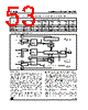
50 / 184 page  9 - CAPTURE/COMPARE (CAPCOM) UNITS ST10F269 50/184 * The CAPCOM2 unit provides 16 capture inputs, but only 12 compare outputs. CC24I to CC27I are inputs only. Figure 13 : Block Diagram of CAPCOM Timers T0 and T7 Figure 14 : Block Diagram of CAPCOM Timers T1 and T8 Note: When an external input signal is connected to the input lines of both T0 and T7, these timers count the input signal synchronously. Thus the two timers can be regarded as one timer whose contents can be compared with 32 capture registers. When a capture/compare register has been selected for capture mode, the current contents of the allocated timer will be latched (captured) into the capture/compare register in response to an external event at the port pin which is associated with this register. In addition, a specific interrupt request for this capture/compare register is generated. Either a positive, a negative, or both a positive and a negative external signal transition at the pin can be selected as the triggering event. The contents of all registers which have been selected for one of the five compare modes are continuously compared with the contents of the allocated timers. When a match occurs between the timer value and the value in a capture /compare register, specific actions will be taken based on the selected compare mode (see Table 9). The input frequencies fTx, for the timer input selector Tx, are determined as a function of the CPU clocks. The timer input frequencies, resolution and periods which result from the selected pre-scaler option in TxI when using a 40MHz CPU clock on PQFP144 devices (or a 32MHz CPU clock on TQFP144 devices) are listed in Table 10 and Table 11 . The numbers for the timer periods are based on a reload value of 0000h. Note that some numbers may be rounded to 3 significant figures. Pin X Txl CPU Clock TxR MUX GPT2 Timer T6 Over / Underflow Edge Select TxIN Txl Txl TxM Input Control Reload Register TxREL CAPCOM Timer Tx TxIR Interrupt Request x = 0, 7 X Txl CPU Clock TxR MUX GPT2 Timer T6 Over / Underflow TxM Reload Register TxREL CAPCOM Timer Tx TxIR Interrupt Request x = 1, 8 |
|
Lien URL |
| ALLDATASHEET vous a-t-il été utile ? [ DONATE ] |
À propos de Alldatasheet | Publicité | Contactez-nous | Politique de confidentialité | Lien vers la fiche technique | Echange de liens | Fabricants All Rights Reserved©Alldatasheet.com |
| Russian : Alldatasheetru.com | Korean : Alldatasheet.co.kr | Spanish : Alldatasheet.es | French : Alldatasheet.fr | Italian : Alldatasheetit.com Portuguese : Alldatasheetpt.com | Polish : Alldatasheet.pl | Vietnamese : Alldatasheet.vn Indian : Alldatasheet.in | Mexican : Alldatasheet.com.mx | British : Alldatasheet.co.uk | New Zealand : Alldatasheet.co.nz |
|
Family Site : ic2ic.com |
icmetro.com |
 French ▼
 English
 Chinese
 German
 Japanese
 Russian
 Korean
 Spanish
 French
 Italian
 Portuguese
 Polish
 Vietnamese
 Indian
 Mexican
 British
 New Zealand