|
Moteur de recherche de fiches techniques de composants électroniques |
|
|
Moteur de recherche de fiches techniques de composants électroniques |
|
ST10F269Z1Q3 Fiches technique(PDF) 92 Page - STMicroelectronics |
|
|
|||||||||||||||||||||||||||||
ST10F269Z1Q3 Fiches technique(HTML) 92 Page - STMicroelectronics |
|
|
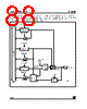
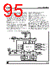
92 / 184 page  12 - PARALLEL PORTS ST10F269 92/184 The structure of Port 8 differs in the way the output latches are connected to the internal bus and to the pin driver (see Figure 43). Pins P8.7...P8.0 (CC23IO...CC16IO) combine internal bus data and alternate data output before the port latch input, as do the Port 2 pins. Figure 43 : Block Diagram of Port 8 Pins P8.7...P8.0 Open Drain Latch Write ODP8.y Read ODP8.y Direction Latch Write DP8.y Read DP8.y MUX 0 1 Alternate Latch Data Input Input Latch Clock P8.y CCzIO Output Buffer Alternate Data Output MUX 0 1 Output Latch ≥ 1 Write Port P8.y Compare Trigger Read P8.y y = (7...0) z = (16...23) Alternate Pin Data Input |
|
Lien URL |
| ALLDATASHEET vous a-t-il été utile ? [ DONATE ] |
À propos de Alldatasheet | Publicité | Contactez-nous | Politique de confidentialité | Lien vers la fiche technique | Echange de liens | Fabricants All Rights Reserved©Alldatasheet.com |
| Russian : Alldatasheetru.com | Korean : Alldatasheet.co.kr | Spanish : Alldatasheet.es | French : Alldatasheet.fr | Italian : Alldatasheetit.com Portuguese : Alldatasheetpt.com | Polish : Alldatasheet.pl | Vietnamese : Alldatasheet.vn Indian : Alldatasheet.in | Mexican : Alldatasheet.com.mx | British : Alldatasheet.co.uk | New Zealand : Alldatasheet.co.nz |
|
Family Site : ic2ic.com |
icmetro.com |
 French ▼
 English
 Chinese
 German
 Japanese
 Russian
 Korean
 Spanish
 French
 Italian
 Portuguese
 Polish
 Vietnamese
 Indian
 Mexican
 British
 New Zealand