|
Moteur de recherche de fiches techniques de composants électroniques |
|
|
Moteur de recherche de fiches techniques de composants électroniques |
|
STM32F745ZE Fiches technique(PDF) 152 Page - STMicroelectronics |
|
|
|||||||||||||||||||||||||||||
STM32F745ZE Fiches technique(HTML) 152 Page - STMicroelectronics |
|
|
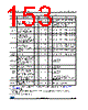
152 / 227 page  Electrical characteristics STM32F745xx STM32F746xx 152/227 DocID027590 Rev 4 5.3.25 DAC electrical characteristics TCoeff(2) Temperature coefficient - - 30 50 ppm/°C tSTART(2) Startup time - - 6 10 µs 1. Shortest sampling time can be determined in the application by multiple iterations. 2. Guaranteed by design. Table 71. internal reference voltage (continued) Symbol Parameter Conditions Min Typ Max Unit Table 72. Internal reference voltage calibration values Symbol Parameter Memory address VREFIN_CAL Raw data acquired at temperature of 30 °C VDDA = 3.3 V 0x1FF0 F44A - 0x1FF0 F44B Table 73. DAC characteristics Symbol Parameter Min Typ Max Unit Comments VDDA Analog supply voltage 1.7(1) -3.6 V - VREF+ Reference supply voltage 1.7(1) -3.6 V VREF+ ≤VDDA VSSA Ground 0- 0V - RLOAD(2) Resistive load with buffer ON 5 - - k Ω - RO(2) Impedance output with buffer OFF -- 15 k Ω When the buffer is OFF, the Minimum resistive load between DAC_OUT and VSS to have a 1% accuracy is 1.5 MΩ CLOAD(2) Capacitive load - - 50 pF Maximum capacitive load at DAC_OUT pin (when the buffer is ON). DAC_OUT min(2) Lower DAC_OUT voltage with buffer ON 0.2 - - V It gives the maximum output excursion of the DAC. It corresponds to 12-bit input code (0x0E0) to (0xF1C) at VREF+ = 3.6 V and (0x1C7) to (0xE38) at VREF+ = 1.7 V DAC_OUT max(2) Higher DAC_OUT voltage with buffer ON -- VDDA − 0.2 V DAC_OUT min(2) Lower DAC_OUT voltage with buffer OFF -0.5 - mV It gives the maximum output excursion of the DAC. DAC_OUT max(2) Higher DAC_OUT voltage with buffer OFF -- VREF+ − 1LSB V IVREF+(4) DAC DC VREF current consumption in quiescent mode (Standby mode) -170 240 µA With no load, worst code (0x800) at VREF+ = 3.6 V in terms of DC consumption on the inputs -50 75 With no load, worst code (0xF1C) at VREF+ = 3.6 V in terms of DC consumption on the inputs |
|
Lien URL |
| ALLDATASHEET vous a-t-il été utile ? [ DONATE ] |
À propos de Alldatasheet | Publicité | Contactez-nous | Politique de confidentialité | Lien vers la fiche technique | Echange de liens | Fabricants All Rights Reserved©Alldatasheet.com |
| Russian : Alldatasheetru.com | Korean : Alldatasheet.co.kr | Spanish : Alldatasheet.es | French : Alldatasheet.fr | Italian : Alldatasheetit.com Portuguese : Alldatasheetpt.com | Polish : Alldatasheet.pl | Vietnamese : Alldatasheet.vn Indian : Alldatasheet.in | Mexican : Alldatasheet.com.mx | British : Alldatasheet.co.uk | New Zealand : Alldatasheet.co.nz |
|
Family Site : ic2ic.com |
icmetro.com |
 French ▼
 English
 Chinese
 German
 Japanese
 Russian
 Korean
 Spanish
 French
 Italian
 Portuguese
 Polish
 Vietnamese
 Indian
 Mexican
 British
 New Zealand