|
Moteur de recherche de fiches techniques de composants électroniques |
|
|
Moteur de recherche de fiches techniques de composants électroniques |
|
VM800C43A-N Fiches technique(PDF) 9 Page - Future Technology Devices International Ltd. |
|
|
|||||||||||||||||||||||||||||
VM800C43A-N Fiches technique(HTML) 9 Page - Future Technology Devices International Ltd. |
|
|
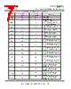
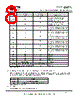
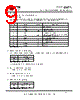
9 / 22 page  9 Copyright © 2013 Future Technology Devices International Limited VM800C Datasheet Version 1.0 Document Reference No.: FT_000844 Clearance No.: FTDI# 345 J4 – SP- Audio speaker -ve from the onboard amplifier. J5- SPI Interface This is the interface where the SPI control and data signals are routed. There are also power and ground pins on this interface. Note J5 is not soldered on the VM800C board by default. Pin No. Name Type Description 1 SCLK I SPI Clock input 2 MOSI I Master Out Slave in 3 MISO O Master In Slave out 4 CS# I Chip select , active low 5 INT# OD Host interrupt open drain output, active low. On board 47k Ω pull-up to 3.3V. 6 PD# I Active low power down input. 7 5V P 5V power supply 8 3.3V P 3.3V power supply 9 GND P Ground 10 GND P Ground Table 3-6 – J5 Pinout JP1- Audio Amplifier Power Select This jumper provides the option to select the power supply voltage for the onboard power amplifier. Pin No. Name 1-2 3V3 selected 2-3 5V selected Table 3-7 – JP1 Pin options *This needs to be configured before audio can be heard JP2 – On board amplifier enable Solder connection fitted by default JP3 - On board amplifier mute Solder connection not fited by default SW1 – Power source select Pin No. Name 1-2 Power from CN1 2-3 Power from CN2 Table 3-8 – JP1 Pin options |
|
|
Lien URL |
| ALLDATASHEET vous a-t-il été utile ? [ DONATE ] |
À propos de Alldatasheet | Publicité | Contactez-nous | Politique de confidentialité | Lien vers la fiche technique | Echange de liens | Fabricants All Rights Reserved©Alldatasheet.com |
| Russian : Alldatasheetru.com | Korean : Alldatasheet.co.kr | Spanish : Alldatasheet.es | French : Alldatasheet.fr | Italian : Alldatasheetit.com Portuguese : Alldatasheetpt.com | Polish : Alldatasheet.pl | Vietnamese : Alldatasheet.vn Indian : Alldatasheet.in | Mexican : Alldatasheet.com.mx | British : Alldatasheet.co.uk | New Zealand : Alldatasheet.co.nz |
|
Family Site : ic2ic.com |
icmetro.com |
 French ▼
 English
 Chinese
 German
 Japanese
 Russian
 Korean
 Spanish
 French
 Italian
 Portuguese
 Polish
 Vietnamese
 Indian
 Mexican
 British
 New Zealand