|
Moteur de recherche de fiches techniques de composants électroniques |
|
|
Moteur de recherche de fiches techniques de composants électroniques |
|
STPCATLAS Fiches technique(PDF) 103 Page - STMicroelectronics |
|
|
|||||||||||||||||||||||||||||
STPCATLAS Fiches technique(HTML) 103 Page - STMicroelectronics |
|
|
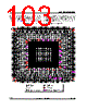
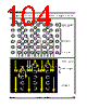
103 / 111 page  DESIGN GUIDELINES Issue 1.0 - July 24, 2002 103/111 As the PCB acts as a heat sink, the layout of top and ground layers must be done with care to maximize the board surface dissipating the heat. The only limitation is the risk of losing routing channels. Figure 6-36 and Figure 6-37 show a routing with a good thermal dissipation thanks to an optimized placement of power and signal vias. The ground plane should be on bottom layer for the best heat spreading (thicker layer than internal ones) and dissipation (direct contact with air). . Figure 6-36. Layout for Good Thermal Dissipation - top layer 1 A 3.3V ball 2.5V ball (Core / PLLs) Via STPC ball GND ball Not Connected ball |
|
Lien URL |
| ALLDATASHEET vous a-t-il été utile ? [ DONATE ] |
À propos de Alldatasheet | Publicité | Contactez-nous | Politique de confidentialité | Lien vers la fiche technique | Echange de liens | Fabricants All Rights Reserved©Alldatasheet.com |
| Russian : Alldatasheetru.com | Korean : Alldatasheet.co.kr | Spanish : Alldatasheet.es | French : Alldatasheet.fr | Italian : Alldatasheetit.com Portuguese : Alldatasheetpt.com | Polish : Alldatasheet.pl | Vietnamese : Alldatasheet.vn Indian : Alldatasheet.in | Mexican : Alldatasheet.com.mx | British : Alldatasheet.co.uk | New Zealand : Alldatasheet.co.nz |
|
Family Site : ic2ic.com |
icmetro.com |
 French ▼
 English
 Chinese
 German
 Japanese
 Russian
 Korean
 Spanish
 French
 Italian
 Portuguese
 Polish
 Vietnamese
 Indian
 Mexican
 British
 New Zealand