|
Moteur de recherche de fiches techniques de composants électroniques |
|
|
Moteur de recherche de fiches techniques de composants électroniques |
|
TL331 Fiches technique(PDF) 2 Page - Texas Instruments |
|
|
|||||||||||||||||||||||||||||
TL331 Fiches technique(HTML) 2 Page - Texas Instruments |
|
|
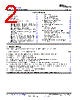
2 / 21 page  2 TL331, TL331B, TL391B SLVS238H – AUGUST 1999 – REVISED MAY 2020 www.ti.com Product Folder Links: TL331 TL331B TL391B Submit Documentation Feedback Copyright © 1999–2020, Texas Instruments Incorporated Table of Contents 1 Features .................................................................. 1 2 Applications ........................................................... 1 3 Description ............................................................. 1 4 Revision History..................................................... 2 5 Pin Configuration and Functions ......................... 3 6 Specifications......................................................... 4 6.1 Absolute Maximum Ratings, TL331 and TL331K ..... 4 6.2 Absolute Maximum Ratings, TL331B and TL391B... 4 6.3 ESD Ratings, TL331 and TL331K............................. 4 6.4 ESD Ratings, TL331B and TL391B .......................... 5 6.5 Recommended Operating Conditions, TL331 and TL331K....................................................................... 5 6.6 Recommended Operating Conditions, TL331B and TL391B....................................................................... 5 6.7 Thermal Information .................................................. 5 6.8 Electrical Characteristics, TL331B and TL391B ....... 6 6.9 Switching Characteristics, TL331B and TL391B....... 6 6.10 Electrical Characteristics, TL331 and TL331K........ 7 6.11 Switching Characteristics, TL331 and TL331K ....... 7 6.12 Typical Characteristics, TL331 and TL331K ........... 8 7 Detailed Description .............................................. 9 7.1 Overview ................................................................... 9 7.2 Functional Block Diagram ......................................... 9 7.3 Feature Description................................................... 9 7.4 Device Functional Modes.......................................... 9 8 Application and Implementation ........................ 10 8.1 Application Information............................................ 10 8.2 Typical Application ................................................. 10 9 Power Supply Recommendations ...................... 12 10 Layout................................................................... 12 10.1 Layout Guidelines ................................................. 12 10.2 Layout Example .................................................... 12 11 Device and Documentation Support ................. 13 11.1 Documentation Support ........................................ 13 11.2 Receiving Notification of Documentation Updates 13 11.3 Community Resources.......................................... 13 11.4 Trademarks ........................................................... 13 11.5 Electrostatic Discharge Caution ............................ 13 11.6 Glossary ................................................................ 13 12 Mechanical, Packaging, and Orderable Information ........................................................... 13 4 Revision History NOTE: Page numbers for previous revisions may differ from page numbers in the current version. Changes from Revision G (January 2015) to Revision H Page • Added TL331B and TL391B tables and pinouts, Updated front page for new B devices for APL......................................... 1 • Added Family Comparison Table to Front Page .................................................................................................................... 1 • Added Input current, IIK in Absolute Maximum Ratings.......................................................................................................... 4 • Changed incorrect TL331 and TL331K Temp Ranges in Recommended Operating Conditions .......................................... 5 • Changed text from: open-drain output to: open-collector output ........................................................................................... 9 • Removed sentence: This is enables much head room for modern day supplies of 3.3 V and 5.0 V. .................................. 9 • Changed the text 'The output NPN will sink current when the positive input voltage is higher than the negative input voltage and the offset voltage' to 'The output NPN will sink current when the negative input voltage is higher than the positive input voltage and the offset voltage.'................................................................................................................... 9 • Changed Output Current specifications from: to: in Design Parameters ............................................................................. 10 • Changed first paragraph of the Response Time section ..................................................................................................... 11 • Added Receiving Notification of Documentation Updates section and Community Resources section .............................. 13 |
|
|
Lien URL |
| ALLDATASHEET vous a-t-il été utile ? [ DONATE ] |
À propos de Alldatasheet | Publicité | Contactez-nous | Politique de confidentialité | Lien vers la fiche technique | Echange de liens | Fabricants All Rights Reserved©Alldatasheet.com |
| Russian : Alldatasheetru.com | Korean : Alldatasheet.co.kr | Spanish : Alldatasheet.es | French : Alldatasheet.fr | Italian : Alldatasheetit.com Portuguese : Alldatasheetpt.com | Polish : Alldatasheet.pl | Vietnamese : Alldatasheet.vn Indian : Alldatasheet.in | Mexican : Alldatasheet.com.mx | British : Alldatasheet.co.uk | New Zealand : Alldatasheet.co.nz |
|
Family Site : ic2ic.com |
icmetro.com |
 French ▼
 English
 Chinese
 German
 Japanese
 Russian
 Korean
 Spanish
 French
 Italian
 Portuguese
 Polish
 Vietnamese
 Indian
 Mexican
 British
 New Zealand