|
Moteur de recherche de fiches techniques de composants électroniques |
|
|
Moteur de recherche de fiches techniques de composants électroniques |
|
LT6556IGN Fiches technique(PDF) 9 Page - Linear Technology |
|
|
|||||||||||||||||||||||||||||
LT6556IGN Fiches technique(HTML) 9 Page - Linear Technology |
|
|
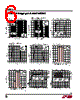
9 / 16 page  LT6556 9 6556f To improve clamping, the pin’s DC impedance should be minimized by connecting the VREF pin directly to ground in the symmetric dual supply case with a common mode voltage of 0V. If the common mode voltage is not centered at ground or the input voltage exceeds plus or minus three diodes from ground, an external resistor to either supply can be added to shift the VREF voltage to the desired level. The only way to cover the full input voltage range of V– + 1V to V+ – 1V is to shift VREF up or down. The VREF pin can also be directly driven with a DC source. Figure 2 shows the effect of the clamp on input current when sweeping input voltage with various VREF pin volt- ages. Bypassing the VREF pin is not necessary. INPUT VOLTAGE (V) –4 0 100 4 6556 F02 –100 –250 –200 –2 0 2 –3 –1 1 3 250 200 –50 50 –150 150 TA = 25°C VS = ±5V VREF = 2V VREF = 1V VREF = 0V VREF = –1V VREF = –2V The inputs can be driven beyond the point at which the output clips so long as input currents are limited to less than ±10mA. Continuing to drive the input beyond the output limit can result in increased current drive and slightly increased swing, but will also increase supply current and may result in delays in transient response at larger levels of overdrive. Layout and Grounding It is imperative that care is taken in PCB layout in order to benefit from the very high speed and very low crosstalk of the LT6556. Separate power and ground planes are highly recommended and trace lengths should be kept as short as possible. If input traces must be run over a distance of several centimeters, they should use a controlled imped- ance with either series or shunt terminations (nominally 50Ω or 75Ω) to maintain signal fidelity. Care should be taken to minimize capacitance on the LT6556’s output traces by increasing spacing between traces and adjacent metal and by eliminating metal planes in underlying layers. To drive cable or traces longer than several centimeters, using the LT6555 with its fixed gain of+2 in conjunction with series and load termination resis- tors may provide better results. A plot of AC performance driving a 1k load with various trace lengths is shown in Figure 3. All data is from a 4-layer board with 2oz copper, 18mil of board layer thickness to the ground plane, a trace width of 12mils and spacing to adjacent metal of 18mils. The 0.2cm output trace places the 1k resistor as close to the part as possible, while the other curves show the load resistor consecutively further away. The worst case, 4cm, trace has almost 10pF of parasitic capacitance. FREQUENCY (MHz) 0.1 6 4 2 0 –2 –4 –6 1 10 100 1000 6556 F03 4cm TRACE 0.2cm TRACE 2cm TRACE VS = ±5V VOUT = 200mVP-P RL = 1k TA = 25°C Figure 3. Response vs Output Trace Length APPLICATIO S I FOR ATIO Figure 2. Input Current vs Input Voltage at Different VREF Voltages |
|
|
Lien URL |
| ALLDATASHEET vous a-t-il été utile ? [ DONATE ] |
À propos de Alldatasheet | Publicité | Contactez-nous | Politique de confidentialité | Lien vers la fiche technique | Echange de liens | Fabricants All Rights Reserved©Alldatasheet.com |
| Russian : Alldatasheetru.com | Korean : Alldatasheet.co.kr | Spanish : Alldatasheet.es | French : Alldatasheet.fr | Italian : Alldatasheetit.com Portuguese : Alldatasheetpt.com | Polish : Alldatasheet.pl | Vietnamese : Alldatasheet.vn Indian : Alldatasheet.in | Mexican : Alldatasheet.com.mx | British : Alldatasheet.co.uk | New Zealand : Alldatasheet.co.nz |
|
Family Site : ic2ic.com |
icmetro.com |
 French ▼
 English
 Chinese
 German
 Japanese
 Russian
 Korean
 Spanish
 French
 Italian
 Portuguese
 Polish
 Vietnamese
 Indian
 Mexican
 British
 New Zealand