|
Moteur de recherche de fiches techniques de composants électroniques |
|
|
Moteur de recherche de fiches techniques de composants électroniques |
|
MM1111 Fiches technique(PDF) 9 Page - Mitsumi Electronics, Corp. |
|
|
|||||||||||||||||||||||||||||
MM1111 Fiches technique(HTML) 9 Page - Mitsumi Electronics, Corp. |
|
|
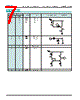
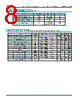
9 / 10 page  MITSUMI 2-Input 1-Output Video Switch / 3-Input 1-Output Video Switch MM1111~MM1118 Measuring Procedures (Except where noted otherwise, VCC=5.0V, VC1=VCC, VC2=0V) Item Symbol Switch state Measuring Procedure S1 S2 S3 S4 S5 Consumption Id 22222 current 12222 Voltage gain GV 21212 22111 22121 12222 Frequency FC 21212 characteristic 22111 22121 12222 Differential gain DG 21212 22111 22121 12222 Differential phase DP 21212 22111 22121 Output offset 22222 voltage Voff 22212 22211 12212 12221 12211 Crosstalk CT 21222 21221 21211 22122 22112 Switch 1 input 22212 voltage H VIH1 Switch 1 input voltage L VIL1 Switch 2 input 22221 voltage H VIH2 Switch 2 input voltage L VIL2 Connect a DC ammeter to the VCC pin and measure. The ammeter is shorted for use in subsequent measurements. Input a 1.0VP-P, 100kHz sine wave to SG, and obtain GV from the following formula given TP1 voltage as V1 and TP3 voltage as V2. GV=20LOG (V2/V1) dB For the above GV measurement, given TP3 voltage for 10MHz as V3, FC is obtained from the following formula. FC=20LOG (V3/V2) dB Input a 1.0VP-P staircase wave to SG, and measure differential gain at TP3. APL=10~90% Proceed as for DG, and measure differential phase. Measure the DC voltage difference of each switch status at TP2. Assume VC1=2.1V, VC2=0.7V. Input a 2.0VP-P, 4.43MHz sine wave to SG, and given TP1 voltage as V4 and TP3 voltage as V5, CT is obtained from the following formula. CT = 20LOG (V5/V4) dB Impress an optional DC voltage on TP6 and TP7. Gradually raise from VC1=0V. TP4 voltage when TP7 voltage is output on TP2 is VIH1. Gradually lower from VC1=VCC. TP4 voltage when TP6 voltage is output on TP2 is VIL1. Impress an optional DC voltage on TP6 and TP8. Gradually raise from VC1=0V. TP5 voltage when TP8 voltage is output on TP2 is VIH2. Gradually lower from VC1=VCC. TP5 voltage when TP6 voltage is output on TP2 is VIL2. |
|
|
Lien URL |
| ALLDATASHEET vous a-t-il été utile ? [ DONATE ] |
À propos de Alldatasheet | Publicité | Contactez-nous | Politique de confidentialité | Lien vers la fiche technique | Echange de liens | Fabricants All Rights Reserved©Alldatasheet.com |
| Russian : Alldatasheetru.com | Korean : Alldatasheet.co.kr | Spanish : Alldatasheet.es | French : Alldatasheet.fr | Italian : Alldatasheetit.com Portuguese : Alldatasheetpt.com | Polish : Alldatasheet.pl | Vietnamese : Alldatasheet.vn Indian : Alldatasheet.in | Mexican : Alldatasheet.com.mx | British : Alldatasheet.co.uk | New Zealand : Alldatasheet.co.nz |
|
Family Site : ic2ic.com |
icmetro.com |
 French ▼
 English
 Chinese
 German
 Japanese
 Russian
 Korean
 Spanish
 French
 Italian
 Portuguese
 Polish
 Vietnamese
 Indian
 Mexican
 British
 New Zealand