|
Moteur de recherche de fiches techniques de composants électroniques |
|
|
Moteur de recherche de fiches techniques de composants électroniques |
|
AD6623BC/PCB Fiches technique(PDF) 14 Page - Analog Devices |
|
|
|||||||||||||||||||||||||||||
AD6623BC/PCB Fiches technique(HTML) 14 Page - Analog Devices |
|
|
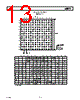
14 / 40 page  REV. 0 AD6623 –14– 196-PIN FUNCTION DESCRIPTIONS Mnemonic Type Function POWER SUPPLY VDD P 2.5 V Supply VDDIO P 3.3 V IO Supply GND G Ground INPUTS INOUT[17:0] 1 I/O A Input Data (Mantissa) QIN 1 I When HIGH Indicates Q Input Data (Complex Input Mode) RESET2 I Active LOW Reset Pin CLK 1 I Input Clock SYNC0 1 I All Sync Pins Go to All Four Output Channels SYNC1 1 I All Sync Pins Go to All Four Output Channels SYNC2 1 I All Sync Pins Go to All Four Output Channels SYNC3 1 I All Sync Pins Go to All Four Output Channels SDINA 1 I Serial Data Input—Channel A SDINB 1 I Serial Data Input—Channel B SDINC 1 I Serial Data Input—Channel C SDIND 1 I Serial Data Input—Channel D CS I Active LOW Chip Select CONTROL SCLKA I/O Bidirectional Serial Clock—Channel A SCLKB I/O Bidirectional Serial Clock—Channel B SCLKC I/O Bidirectional Serial Clock—Channel C SCLKD I/O Bidirectional Serial Clock—Channel D SDFOA O Serial Data Frame Sync Output—Channel A SDFOB O Serial Data Frame Sync Output—Channel B SDFOC O Serial Data Frame Sync Output—Channel C SDFOD O Serial Data Frame Sync Output—Channel D SDFIA I Serial Data Frame Input—Channel A SDFIB I Serial Data Frame Input—Channel B SDFIC I Serial Data Frame Input—Channel C SDFID I Serial Data Frame Input—Channel D OEN 1 I Active High Output Enable Pin MICROPORT CONTROL D[7:0] I/O/T Bidirectional Microport Data A[2:0] I Microport Address Bus DS (RD) I Active Low Data Strobe (Active Low Read) DTACK (RDY)2 O/T Active Low Data Acknowledge (Microport Status Bit) RW ( WR) I Read Write (Active Low Write) MODE I Intel or Motorola Mode Select OUTPUTS OUT[17:0] O Wideband Output Data QOUT O When HIGH Indicates Q Output Data (Complex Output Mode) JTAG AND BIST TRST2 I Test Reset Pin (Active Low) TCK1 I Test Clock Input TMS 2 I Test Mode Select Input TDO O/T Test Data Output TDI1 I Test Data Input NOTES 1Pins with a Pull-Down resistor of nominal 70 k Ω. 2Pins with a Pull-Up resistors of nominal 70 k Ω. |
|
Lien URL |
| ALLDATASHEET vous a-t-il été utile ? [ DONATE ] |
À propos de Alldatasheet | Publicité | Contactez-nous | Politique de confidentialité | Lien vers la fiche technique | Echange de liens | Fabricants All Rights Reserved©Alldatasheet.com |
| Russian : Alldatasheetru.com | Korean : Alldatasheet.co.kr | Spanish : Alldatasheet.es | French : Alldatasheet.fr | Italian : Alldatasheetit.com Portuguese : Alldatasheetpt.com | Polish : Alldatasheet.pl | Vietnamese : Alldatasheet.vn Indian : Alldatasheet.in | Mexican : Alldatasheet.com.mx | British : Alldatasheet.co.uk | New Zealand : Alldatasheet.co.nz |
|
Family Site : ic2ic.com |
icmetro.com |
 French ▼
 English
 Chinese
 German
 Japanese
 Russian
 Korean
 Spanish
 French
 Italian
 Portuguese
 Polish
 Vietnamese
 Indian
 Mexican
 British
 New Zealand