|
Moteur de recherche de fiches techniques de composants électroniques |
|
|
Moteur de recherche de fiches techniques de composants électroniques |
|
AD8295BCPZ-R7 Fiches technique(PDF) 21 Page - Analog Devices |
|
|
|||||||||||||||||||||||||||||
AD8295BCPZ-R7 Fiches technique(HTML) 21 Page - Analog Devices |
|
|
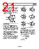
21 / 28 page  AD8295 Rev. 0 | Page 21 of 2 8 Power Supplies A stable dc voltage should be used to power the instrumentation amplifier. Noise on the supply pins can adversely affect perfor- mance. See the PSRR performance curves in Figure 14 and Figure 15 for more information. A 0.1 μF capacitor should be placed as close as possible to each supply pin. An additional capacitor, a 10 μF tantalum for the lower frequencies, can be used farther away from the IC. In most cases, the 10 μF bypass capacitor can be shared by other integrated circuits on the same PCB. AD8295 IN-AMP +VS +IN RG –IN LOAD REF 0.1µF 10µF 0.1µF 10µF –VS VOUT Figure 55. Supply Decoupling, REF, and Output Referred to Local Ground INPUT PROTECTION All terminals of the AD8295 are protected against ESD by diodes at the inputs. If voltages beyond the supplies are anticipated, resistors should be placed in series with the inputs to limit the current. Resistors should be chosen so that current does not exceed 6 mA into the internal ESD diodes in the over- load condition. These resistors can be the same as those used for RFI protection. (See the RF Interference section for more information.) For applications where the AD8295 encounters extreme overload voltages, as in cardiac defibrillators, external series resistors and low leakage diode clamps, such as BAV199Ls, FJH1100s, or SP720s can be used. INPUT BIAS CURRENT RETURN PATH The input bias currents of the AD8295 must have a return path to common. When the source, such as a thermocouple, cannot provide a return current path, one should be created, as shown in Figure 56. Otherwise, the input currents charge up the input capacitance until the in-amp is turned off or saturated. THERMOCOUPLE +VS REF –VS CAPACITIVELY COUPLED +VS REF C C –VS AD8295 IN-AMP AD8295 IN-AMP TRANSFORMER +VS REF –VS INCORRECT CAPACITIVELY COUPLED +VS REF C R R C –VS AD8295 IN-AMP 1 fHIGH-PASS = 2πRC THERMOCOUPLE +VS REF –VS 10MΩ TRANSFORMER +VS REF –VS CORRECT AD8295 IN-AMP AD8295 IN-AMP AD8295 IN-AMP Figure 56. Creating an Input Bias Current Return Path RF INTERFERENCE RF interference is often a problem when amplifiers are used in applications where there are strong RF signals. The precision circuits in the AD8295 can rectify the RF signals so that they appear as a dc offset voltage error. To avoid this rectification, place a low-pass filter before the input. Figure 57 shows such a network in front of the instrumentation amplifier. The filter limits both the differential and common-mode bandwidth, as shown in the following equations: ) 2 ( π 2 1 ) ( C D FILTER C C R Diff f + = C FILTER RC CM f π 2 1 ) ( = where CD ≥ 10CC. |
|
Lien URL |
| ALLDATASHEET vous a-t-il été utile ? [ DONATE ] |
À propos de Alldatasheet | Publicité | Contactez-nous | Politique de confidentialité | Lien vers la fiche technique | Echange de liens | Fabricants All Rights Reserved©Alldatasheet.com |
| Russian : Alldatasheetru.com | Korean : Alldatasheet.co.kr | Spanish : Alldatasheet.es | French : Alldatasheet.fr | Italian : Alldatasheetit.com Portuguese : Alldatasheetpt.com | Polish : Alldatasheet.pl | Vietnamese : Alldatasheet.vn Indian : Alldatasheet.in | Mexican : Alldatasheet.com.mx | British : Alldatasheet.co.uk | New Zealand : Alldatasheet.co.nz |
|
Family Site : ic2ic.com |
icmetro.com |
 French ▼
 English
 Chinese
 German
 Japanese
 Russian
 Korean
 Spanish
 French
 Italian
 Portuguese
 Polish
 Vietnamese
 Indian
 Mexican
 British
 New Zealand