|
Moteur de recherche de fiches techniques de composants électroniques |
|
|
Moteur de recherche de fiches techniques de composants électroniques |
|
ADG774ABCPZ-R2 Fiches technique(PDF) 11 Page - Analog Devices |
|
|
|||||||||||||||||||||||||||||
ADG774ABCPZ-R2 Fiches technique(HTML) 11 Page - Analog Devices |
|
|
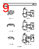
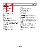
11 / 14 page  Data Sheet ADG774A Rev. C | Page 11 of 14 TERMINOLOGY VDD Most positive power supply potential. GND Ground (0 V) reference. S Source terminal. May be an input or output. D Drain terminal. May be an input or output. IN Logic control input. EN Logic control input. RON Ohmic resistance between D and S. ∆RON On resistance match between any two channels, that is, RON max − RON min. RFLAT(ON) Flatness is defined as the difference between the maximum and minimum value of on resistance as measured over the specified analog signal range. IS (OFF) Source leakage current with the switch off. ID (OFF) Drain leakage current with the switch off. ID, IS (ON) Channel leakage current with the switch on. VD (VS) Analog voltage on the D and S terminals. CS (OFF) Off switch source capacitance. CD (OFF) Off switch drain capacitance. CD, CS (ON) On switch capacitance. tON Delay between applying the digital control input and the output switching on. See Figure 22. tOFF Delay between applying the digital control input and the output switching off. tD Off time or on time measured between the 80% points of both switches when switching from one address state to another. See Figure 23. Crosstalk A measure of unwanted signal that is coupled through from one channel to another because of parasitic capacitance. Off Isolation A measure of unwanted signal coupling through an off switch. Bandwidth Frequency response of the switch in the on state measured at 3 dB down. Distortion RFLAT(ON)/RL |
|
|
Lien URL |
| ALLDATASHEET vous a-t-il été utile ? [ DONATE ] |
À propos de Alldatasheet | Publicité | Contactez-nous | Politique de confidentialité | Lien vers la fiche technique | Echange de liens | Fabricants All Rights Reserved©Alldatasheet.com |
| Russian : Alldatasheetru.com | Korean : Alldatasheet.co.kr | Spanish : Alldatasheet.es | French : Alldatasheet.fr | Italian : Alldatasheetit.com Portuguese : Alldatasheetpt.com | Polish : Alldatasheet.pl | Vietnamese : Alldatasheet.vn Indian : Alldatasheet.in | Mexican : Alldatasheet.com.mx | British : Alldatasheet.co.uk | New Zealand : Alldatasheet.co.nz |
|
Family Site : ic2ic.com |
icmetro.com |
 French ▼
 English
 Chinese
 German
 Japanese
 Russian
 Korean
 Spanish
 French
 Italian
 Portuguese
 Polish
 Vietnamese
 Indian
 Mexican
 British
 New Zealand