 |
Moteur de recherche de fiches techniques de composants électroniques |
|
|
Moteur de recherche de fiches techniques de composants électroniques |
|
The question interval is too short.
Please try again in a few seconds.

Hello, Please ask a question about M24C08-125 Datasheet
# Example questions:
➢ How does the device determine whether to respond to a communication on the i²c bus, and what role do the chip enable (e0, e1, e2) inputs play in this process?
➢ Explain the difference between a random address read and a current address read operation, and under what circumstances would you use each?
➢ What is the purpose of the acknowledge bit (ack) in the i²c protocol, and what action does a device take if it does not receive an ack?
| Part No. | M24C08-125 |
| Manufacturer | STMICROELECTRONICS |
| Size | 261 Kbytes |
| Pages | 30 pages |
| Description | Automotive 16-Kbit, 8-Kbit, 4-Kbit and 2-Kbit serial I²C bus EEPROM |

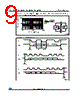
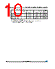
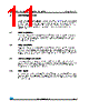

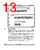






Okay, here's a summary of the provided text, focusing on the key information about the M24C16/C08/C04/C02 EEPROM devices:
Core Functionality:
️· I²C EEPROM: These are electrically erasable programmable read-only memory devices that communicate using the I²C serial communication protocol.
️· Memory Sizes: Available in various sizes: 2kb (M24C02), 4kb (M24C04), 8kb (M24C08), and 16kb (M24C16).
Communication & Addressing:
️· I²C Protocol: Devices operate as slaves on the I²C bus, responding to commands from a master.
️· Device Select Code: Each device is uniquely addressed using a 7-bit code: 4 bits identify the device type, and 3 bits are determined by the state of the E0, E1, and E2 pins (Chip Enable). This allows up to 8 M24C02, 4 M24C04, 2 M24C08 or 1 M24C16 devices to share a single I²C bus.
️· Read/Write Bit (RW): The RW bit is used to indicate a read (RW=1) or write (RW=0) operation.
️· Addressing Modes: Supports current address read, random address read, sequential read, and byte/page write operations.
Key Operating Concepts:
️· Start/Stop Conditions: I²C communication begins with a Start condition (falling edge of SDA while SCL is high) and ends with a Stop condition (rising edge of SDA while SCL is high).
️· Acknowledge (ACK): Used to confirm successful data transfer between devices.
️· Data Input: Data is sampled on the rising edge of the clock (SCL).
Important Pins/Signals:
️· SDA (Serial Data): Used for both sending and receiving data.
️· SCL (Serial Clock): Provides the clock signal for synchronization.
️· E0, E1, E2 (Chip Enable): Used as the 3-bit Chip Enable address for unique device selection on the I2C bus.
In essence, this document provides a technical overview of how to interface with and control these I²C EEPROM devices.
Core Functionality:
️· I²C EEPROM: These are electrically erasable programmable read-only memory devices that communicate using the I²C serial communication protocol.
️· Memory Sizes: Available in various sizes: 2kb (M24C02), 4kb (M24C04), 8kb (M24C08), and 16kb (M24C16).
Communication & Addressing:
️· I²C Protocol: Devices operate as slaves on the I²C bus, responding to commands from a master.
️· Device Select Code: Each device is uniquely addressed using a 7-bit code: 4 bits identify the device type, and 3 bits are determined by the state of the E0, E1, and E2 pins (Chip Enable). This allows up to 8 M24C02, 4 M24C04, 2 M24C08 or 1 M24C16 devices to share a single I²C bus.
️· Read/Write Bit (RW): The RW bit is used to indicate a read (RW=1) or write (RW=0) operation.
️· Addressing Modes: Supports current address read, random address read, sequential read, and byte/page write operations.
Key Operating Concepts:
️· Start/Stop Conditions: I²C communication begins with a Start condition (falling edge of SDA while SCL is high) and ends with a Stop condition (rising edge of SDA while SCL is high).
️· Acknowledge (ACK): Used to confirm successful data transfer between devices.
️· Data Input: Data is sampled on the rising edge of the clock (SCL).
Important Pins/Signals:
️· SDA (Serial Data): Used for both sending and receiving data.
️· SCL (Serial Clock): Provides the clock signal for synchronization.
️· E0, E1, E2 (Chip Enable): Used as the 3-bit Chip Enable address for unique device selection on the I2C bus.
In essence, this document provides a technical overview of how to interface with and control these I²C EEPROM devices.
| Part No. | M24C08-125 |
| Manufacturer | STMICROELECTRONICS |
| Size | 261 Kbytes |
| Pages | 30 pages |
| Description | Automotive 16-Kbit, 8-Kbit, 4-Kbit and 2-Kbit serial I²C bus EEPROM |
| ALLDATASHEET vous a-t-il été utile ? [ DONATE ] |
À propos de Alldatasheet | Publicité | Contactez-nous | Politique de confidentialité | Lien vers la fiche technique | Echange de liens | Fabricants All Rights Reserved©Alldatasheet.com |
| Russian : Alldatasheetru.com | Korean : Alldatasheet.co.kr | Spanish : Alldatasheet.es | French : Alldatasheet.fr | Italian : Alldatasheetit.com Portuguese : Alldatasheetpt.com | Polish : Alldatasheet.pl | Vietnamese : Alldatasheet.vn Indian : Alldatasheet.in | Mexican : Alldatasheet.com.mx | British : Alldatasheet.co.uk | New Zealand : Alldatasheet.co.nz |
|
Family Site : ic2ic.com |
icmetro.com |
 French ▼
  English
 Chinese
 German
 Japanese
 Russian
 Korean
 Spanish
 Italian
 Portuguese
 Polish
 Vietnamese
 Indian
 Mexican
 British
 New Zealand