|
Moteur de recherche de fiches techniques de composants électroniques |
|
|
Moteur de recherche de fiches techniques de composants électroniques |
|
LM1209 Fiches technique(PDF) 12 Page - National Semiconductor (TI) |
|
|
|
|||||||||||||||||||||||||||||
LM1209 Fiches technique(HTML) 12 Page - National Semiconductor (TI) |
|
|
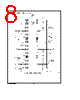
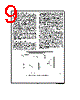
12 / 24 page  Circuit Description (Continued) transistors Note that the bias voltage passes through three diode drops (Q5 Q6 and Q7) before setting the voltage across R9 Q2 Q3 and Q4 also provide three diode drops to the bias voltage at the base of Q5 temperature compen- sating for the diode drops of Q5 Q6 and Q7 This insures that the bias voltage across R9 remains very constant over temperature providing an accurate bias current for the dif- ferential transistor pair Q8 and Q9 thus assuring proper op- eration of the contrast control Q6 serves as a buffer to the input video signal Its emitter drives the base of Q7 Thus the video signal modulates the current flowing through R9 which in turn modulates the cur- rents through the differential pair formed by Q8 and Q9 The current flow through Q8 and Q9 is controlled by a DC volt- age from the Contrast Control circuit This DC voltage is common to all three channels Increasing the voltage to the base of Q9 with respect to the base of Q8 increases the current flow through Q9 A higher current flow through Q9 increases the video gain (contrast) of the LM1208LM1209 Q10 and Q11 also form a differential pair at the collector of Q9 The operation of this differential pair is similar to Q8 and Q9 The DC control voltage is from the Drive Control cir- cuits Each channel has its own drive control circuit In- creasing the voltage to the base of Q11 increases the video gain (drive) of the LM1208LM1209 At a 4V control voltage the gain of the LM1208LM1209 is at maximum with all the current flowing through Q11 If all the current was flowing through Q10 the video signal attenuation would be over 40 dB the maximum attenuation Q12 through Q17 are part of the final section shown in Figure 8 DC restoration is done at this stage The clamp comparator (Figure 11) drives the clamp cap at pin 8 to a voltage that sets the correct black level of the video signal This cap is also connected to the base of Q17 Q17 and Q16 are one half of the darlington differential pair The clamp cap voltage establishes the cur- rent flow through R16 Q15 and R15 With the bases of Q14 and Q15 held to the same voltage the current through Q15 is mirrored into Q14 and the other half of the differen- tial pair Q12 and Q13 By this current mirror the voltage at the collector of Q14 is set to the correct DC value for the video signal by controlling the voltage drop across R13 completing the DC restoration TLH11884 13 FIGURE 8 Simplified Schematic of LM1208LM1209 Video Amplifier Input Stage http www nationalcom 12 |
|
Lien URL |
| ALLDATASHEET vous a-t-il été utile ? [ DONATE ] |
À propos de Alldatasheet | Publicité | Contactez-nous | Politique de confidentialité | Lien vers la fiche technique | Echange de liens | Fabricants All Rights Reserved©Alldatasheet.com |
| Russian : Alldatasheetru.com | Korean : Alldatasheet.co.kr | Spanish : Alldatasheet.es | French : Alldatasheet.fr | Italian : Alldatasheetit.com Portuguese : Alldatasheetpt.com | Polish : Alldatasheet.pl | Vietnamese : Alldatasheet.vn Indian : Alldatasheet.in | Mexican : Alldatasheet.com.mx | British : Alldatasheet.co.uk | New Zealand : Alldatasheet.co.nz |
|
Family Site : ic2ic.com |
icmetro.com |
 French ▼
 English
 Chinese
 German
 Japanese
 Russian
 Korean
 Spanish
 French
 Italian
 Portuguese
 Polish
 Vietnamese
 Indian
 Mexican
 British
 New Zealand