|
Moteur de recherche de fiches techniques de composants électroniques |
|
|
Moteur de recherche de fiches techniques de composants électroniques |
|
ADP1715ARMZ-R7 Fiches technique(PDF) 15 Page - Analog Devices |
|
|
|||||||||||||||||||||||||||||
ADP1715ARMZ-R7 Fiches technique(HTML) 15 Page - Analog Devices |
|
|
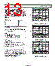
15 / 20 page  ADP1715/ADP1716 Rev. 0 | Page 15 of 20 140 0 0 VIN – VOUT (V) 5 120 100 80 60 40 20 12 34 1mA 10mA 50mA 100mA 250mA 360mA 500mA (LOAD CURRENT) DO NOT OPERATE ABOVE THIS POINT MAX TJ Figure 43. 300 mm2 of PCB Copper, TA = 85°C 140 0 05 VIN – VOUT (V) 120 100 80 60 40 20 12 34 1mA 10mA 50mA 100mA 250mA 360mA 500mA (LOAD CURRENT) DO NOT OPERATE ABOVE THIS POINT MAX TJ Figure 44. 100 mm2 of PCB Copper, TA = 85°C 140 0 05 VIN – VOUT (V) 120 100 80 60 40 20 12 34 1mA 10mA 50mA 100mA 250mA 360mA 500mA (LOAD CURRENT) DO NOT OPERATE ABOVE THIS POINT MAX TJ Figure 45. 0 mm2 of PCB Copper, TA = 85°C PRINTED CIRCUIT BOARD LAYOUT CONSIDERATIONS The 8-lead MSOP package has the four GND pins fused together internally, which enhances its thermal characteristics. Heat dissipation from the package is increased by connecting as much copper as possible to the four GND pins of the ADP1715/ ADP1716. From Table 5 it can be seen that a point of diminishing returns eventually is reached, beyond which an increase in the copper size does not yield additional heat dissipation benefits. Figure 46 shows a typical layout for the ADP1715/ADP1716. The four GND pins are connected to a large copper pad. If a second layer is available, multiple vias can be used to connect them, increasing the overall copper area. The input capacitor should be placed as close as possible to the IN and GND pins. The output capacitor should be placed as close as possible to the OUT and GND pins. 0603 or 0402 size capacitors and resistors should be used to achieve the smallest possible footprint solution on boards where area is limited. GND (TOP) GND (BOTTOM) C1 C2 C3 R2 R1 EN IN OUT ADP1715/ ADP1716 Figure 46. Example PCB Layout |
|
|
Lien URL |
| ALLDATASHEET vous a-t-il été utile ? [ DONATE ] |
À propos de Alldatasheet | Publicité | Contactez-nous | Politique de confidentialité | Lien vers la fiche technique | Echange de liens | Fabricants All Rights Reserved©Alldatasheet.com |
| Russian : Alldatasheetru.com | Korean : Alldatasheet.co.kr | Spanish : Alldatasheet.es | French : Alldatasheet.fr | Italian : Alldatasheetit.com Portuguese : Alldatasheetpt.com | Polish : Alldatasheet.pl | Vietnamese : Alldatasheet.vn Indian : Alldatasheet.in | Mexican : Alldatasheet.com.mx | British : Alldatasheet.co.uk | New Zealand : Alldatasheet.co.nz |
|
Family Site : ic2ic.com |
icmetro.com |
 French ▼
 English
 Chinese
 German
 Japanese
 Russian
 Korean
 Spanish
 French
 Italian
 Portuguese
 Polish
 Vietnamese
 Indian
 Mexican
 British
 New Zealand