|
Moteur de recherche de fiches techniques de composants électroniques |
|
|
Moteur de recherche de fiches techniques de composants électroniques |
|
AD6620S/PCB Fiches technique(PDF) 32 Page - Analog Devices |
|
|
|||||||||||||||||||||||||||||
AD6620S/PCB Fiches technique(HTML) 32 Page - Analog Devices |
|
|
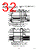
32 / 43 page  AD6620 –32– REV. 0 Mode = 0 If MODE is low during the access, the interface is in Mode 0. In Mode 0 the CS, RD and the WR lines control the access type. While an access is being performed, or if the serial port is DATA VALID tHC tSC tHC tSC tHM ADDRESS VALID N N+1 N+2 N+3 N* CLK1 WR2 RD2 CS3 D[7:0] RDY A[2:0] NOTES: 1 RDY IS DRIVEN LOW ASYNCHRONOUSLY BY WR AND CS GOING LOW AND RETURNS HIGH ON THE RISING EDGE OF CLK "N+2". 2 THESE SIGNALS (R/W AND DS) MAY REMAIN IN LOW STATE TO CONTINUE WRITING DATA. 3 CS MUST RETURN TO HIGH STATE AND BE SAMPLED BY CLK (N+3 SHOWN) TO COMPLETE WRITE. * THE NEXT WRITE MAY BE INITIATED ON CLK, N*. tHA tRDY tRDY tSAM tSAM Figure 49. Mode 0 Write (MODE = GND) accessing the chip, the RDY line goes low at the start of the access. When the internal cycle is complete the RDY line is released. tDD DATA VALID tHC tSC tHC tZD tHA tRDY tRDY ADDRESS VALID tSAM tZR N N+1 N+2 N+3 N+4 N CLK1 WR2 RD2 CS3 D[7:0] RDY1 A[2:0] NOTES: 1 RDY IS DRIVEN LOW ASYNCHRONOUSLY BY RD AND CS GOING LOW AND RETURNS HIGH ON THE RISING EDGE OF CLK "N+3" FOR INTERNAL ACCESS (A[2:0] = 000), CLK "N+2" OTHERWISE. 2 THE SIGNAL, WR, MAY REMAIN HIGH AND RD MAY REMAIN LOW TO CONTINUE READ MODE. 3 CS MUST RETURN TO HIGH STATE AND BE SAMPLED BY CLK (N+4 SHOWN) TO COMPLETE READ. Figure 48. Mode 0 Read (MODE = GND) |
|
Lien URL |
| ALLDATASHEET vous a-t-il été utile ? [ DONATE ] |
À propos de Alldatasheet | Publicité | Contactez-nous | Politique de confidentialité | Lien vers la fiche technique | Echange de liens | Fabricants All Rights Reserved©Alldatasheet.com |
| Russian : Alldatasheetru.com | Korean : Alldatasheet.co.kr | Spanish : Alldatasheet.es | French : Alldatasheet.fr | Italian : Alldatasheetit.com Portuguese : Alldatasheetpt.com | Polish : Alldatasheet.pl | Vietnamese : Alldatasheet.vn Indian : Alldatasheet.in | Mexican : Alldatasheet.com.mx | British : Alldatasheet.co.uk | New Zealand : Alldatasheet.co.nz |
|
Family Site : ic2ic.com |
icmetro.com |
 French ▼
 English
 Chinese
 German
 Japanese
 Russian
 Korean
 Spanish
 French
 Italian
 Portuguese
 Polish
 Vietnamese
 Indian
 Mexican
 British
 New Zealand