|
Moteur de recherche de fiches techniques de composants électroniques |
|
|
Moteur de recherche de fiches techniques de composants électroniques |
|
ADP199ACBZ-R7 Fiches technique(PDF) 11 Page - Analog Devices |
|
|
|||||||||||||||||||||||||||||
ADP199ACBZ-R7 Fiches technique(HTML) 11 Page - Analog Devices |
|
|
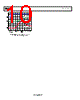
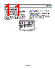
11 / 16 page  Data Sheet ADP199 Rev. 0 | Page 11 of 16 THEORY OF OPERATION The ADP199 is a high-side NMOS load switch controlled by an internal charge pump. The ADP199 is designed to operate with power supply voltages between 0.9 V and 3.6 V. An internal charge pump biases the NMOS switch to achieve a relatively constant, ultralow on resistance of 40 mΩ across the entire input voltage range. The use of the internal charge pump also allows for controlled turn-on times. The switch is controlled on/off by the enable (EN) input and is capable of interfacing directly with 1.2 V logic signals. The ADP199 is capable of 500 mA of continuous load current as long as TJ is less than 85°C. ESD protection structures are shown in the block diagram (see Figure 29) as Zener diodes. The ADP199 is a low quiescent current device with a nominal 4 MΩ pull-down resistor on its enable pin (EN). The package is a space-saving 0.8 mm × 0.8 mm, 4-ball WLCSP. GND EN VIN VOUT ADP199 CHARGE PUMP AND SLEW RATE CONTROL 4Ω Figure 29. Functional Block Diagram |
|
|
Lien URL |
| ALLDATASHEET vous a-t-il été utile ? [ DONATE ] |
À propos de Alldatasheet | Publicité | Contactez-nous | Politique de confidentialité | Lien vers la fiche technique | Echange de liens | Fabricants All Rights Reserved©Alldatasheet.com |
| Russian : Alldatasheetru.com | Korean : Alldatasheet.co.kr | Spanish : Alldatasheet.es | French : Alldatasheet.fr | Italian : Alldatasheetit.com Portuguese : Alldatasheetpt.com | Polish : Alldatasheet.pl | Vietnamese : Alldatasheet.vn Indian : Alldatasheet.in | Mexican : Alldatasheet.com.mx | British : Alldatasheet.co.uk | New Zealand : Alldatasheet.co.nz |
|
Family Site : ic2ic.com |
icmetro.com |
 French ▼
 English
 Chinese
 German
 Japanese
 Russian
 Korean
 Spanish
 French
 Italian
 Portuguese
 Polish
 Vietnamese
 Indian
 Mexican
 British
 New Zealand