|
Moteur de recherche de fiches techniques de composants électroniques |
|
|
Moteur de recherche de fiches techniques de composants électroniques |
|
STA015 Fiches technique(PDF) 22 Page - STMicroelectronics |
|
|
|||||||||||||||||||||||||||||
STA015 Fiches technique(HTML) 22 Page - STMicroelectronics |
|
|
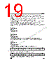
22 / 56 page  Obsolete Product(s) - Obsolete Product(s) STA015 22/56 CMD_INTERRUPT Address: 0x16 (22) Type: R/W Software Reset: 0x00 Hardware Reset: 0x00 X = don’t care; 0 = normal operation; 1 = write into I2C/Ancillary Data The INTERRUPT is used to give STA015 the command to write into the I2C/Ancillary Data Buffer (Regis- ters: 0x7E ... 0xB5). Every time the Master has to extract the new buffer content it writes into this register, setting it to a non-zero value. DATA_REQ_ENABLE Address: 0x18 (24) Type: R/W Software Reset: 0x00 Hardware Reset: 0x00 The DATA_REQ_ENABLE register is used to configure Pin n. 28 working as buffered output clock or data request signal, used for multimedia mode. The buffered Output Clock has the same frequency than the input clock (XTI) SYNCSTATUS Address: 0x40 (64) Type: RO Software Reset: 0x00 Hardware Reset: 0x00 MSB LSB b7 b6 b5 b4 b3 b2 b1 b0 X XXXX XX 0 1 MSB LSB b7 b6 b5 b4 b3 b2 b1 b0 Description XXXX X 0 X X buffered output clock XXXX X 1 X X request signal MSB LSB b7 b6 b5 b4 b3 b2 b1 b0 Description XXXX XX SS1 SS0 0 0 Research of sync word 0 1 Wait for Confirmation 1 0 Synchronised |
|
Lien URL |
| ALLDATASHEET vous a-t-il été utile ? [ DONATE ] |
À propos de Alldatasheet | Publicité | Contactez-nous | Politique de confidentialité | Lien vers la fiche technique | Echange de liens | Fabricants All Rights Reserved©Alldatasheet.com |
| Russian : Alldatasheetru.com | Korean : Alldatasheet.co.kr | Spanish : Alldatasheet.es | French : Alldatasheet.fr | Italian : Alldatasheetit.com Portuguese : Alldatasheetpt.com | Polish : Alldatasheet.pl | Vietnamese : Alldatasheet.vn Indian : Alldatasheet.in | Mexican : Alldatasheet.com.mx | British : Alldatasheet.co.uk | New Zealand : Alldatasheet.co.nz |
|
Family Site : ic2ic.com |
icmetro.com |
 French ▼
 English
 Chinese
 German
 Japanese
 Russian
 Korean
 Spanish
 French
 Italian
 Portuguese
 Polish
 Vietnamese
 Indian
 Mexican
 British
 New Zealand