|
Moteur de recherche de fiches techniques de composants électroniques |
|
|
Moteur de recherche de fiches techniques de composants électroniques |
|
LTC1405IGN Fiches technique(PDF) 7 Page - Linear Technology |
|
|
|||||||||||||||||||||||||||||
LTC1405IGN Fiches technique(HTML) 7 Page - Linear Technology |
|
|
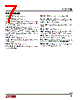
7 / 20 page  7 LTC1405 1405fa PI FU CTIO S +AIN (Pin 1): Positive Analog Input. –AIN (Pin 2): Negative Analog Input. VCM (Pin 3): 2.5V Reference Output.Optional input com- mon mode for single supply operation. Bypass to GND with a 1µF to 10µF ceramic. SENSE (Pin 4): Reference Programming Pin. Ground selects VREF = 4.096V. Short to VREF for 2.048V. Connect SENSE to VDD to drive VREF with an external reference. VREF (Pin 5): DAC Reference. Bypass to GND with a 1µF to 10µF ceramic. GND (Pin 6): DAC Reference Ground. VDD (Pin 7): Analog 5V Supply. Bypass to GND with a 1µF to 10µF ceramic. GND (Pin 8): Analog Power Ground. D11 to D0 (Pins 9 to 20): Data Outputs. The output format is two’s complement. OGND (Pin 21): Output Logic Ground. Tie to GND. OVDD (Pin 22): Positive Supply for the Output Logic. Connect to Pin 23 for 5V logic. If not shorted to Pin 23, bypass to GND with a 1µF ceramic. VDD (Pin 23): Analog 5V Supply. Bypass to GND with a 1µF ceramic. GND (Pin 24): Analog Power Ground. VSS (Pin 25): Negative Supply. Can be – 5V or 0V. If VSS is not shorted to GND, bypass to GND with a 1µF ceramic. CLK (Pin 26): Conversion Start Signal. This active high signal starts a conversion on its rising edge. OF (Pin 27): Overflow Output. This signal is high when the digital output is 011111111111 or 100000000000. GAIN (Pin 28): Gain Select for Input PGA. 5V selects an input gain of 1, 0V selects a gain of 2. |
|
|
Lien URL |
| ALLDATASHEET vous a-t-il été utile ? [ DONATE ] |
À propos de Alldatasheet | Publicité | Contactez-nous | Politique de confidentialité | Lien vers la fiche technique | Echange de liens | Fabricants All Rights Reserved©Alldatasheet.com |
| Russian : Alldatasheetru.com | Korean : Alldatasheet.co.kr | Spanish : Alldatasheet.es | French : Alldatasheet.fr | Italian : Alldatasheetit.com Portuguese : Alldatasheetpt.com | Polish : Alldatasheet.pl | Vietnamese : Alldatasheet.vn Indian : Alldatasheet.in | Mexican : Alldatasheet.com.mx | British : Alldatasheet.co.uk | New Zealand : Alldatasheet.co.nz |
|
Family Site : ic2ic.com |
icmetro.com |
 French ▼
 English
 Chinese
 German
 Japanese
 Russian
 Korean
 Spanish
 French
 Italian
 Portuguese
 Polish
 Vietnamese
 Indian
 Mexican
 British
 New Zealand