CY2300
Document #: 38-07252 Rev. *C
Page 2 of 6
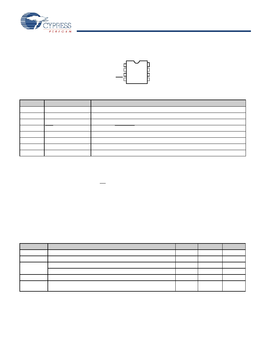
Pinouts
Figure 1. CY2300 -
8-pin SOIC - Top View
Functional Description
The CY2300 is a 4-output 3.3V phase-aligned system clock
designed to distribute high-speed clocks in PC, workstation,
datacom, telecom, and other high-performance applications.
The part allows the user to obtain 1/2x, 1x, 1x and 2x REFIN
output frequencies on respective output pins.
The part has an on-chip PLL which locks to an input clock
presented on the REFIN pin. The input-to-output skew is
guaranteed to be less than
±200 ps, and output-to-output skew
is guaranteed to be less than 200 ps.
Multiple CY2300 devices can accept the same input clock and
distribute it in a system. In this case, the skew between the
outputs of two devices is guaranteed to be less than 400 ps.
The CY2300 is available in commercial temperature range.
Maximum Ratings
Supply Voltage to Ground Potential................–0.5V to +7.0V
DC Input Voltage (Except Ref) .............. –0.5V to VDD + 0.5V
DC Input Voltage REF ........................................... –0.5 to 7V
Storage Temperature ................................. –65°C to +150°C
Junction Temperature ................................................. 150°C
Static Discharge Voltage
(per MIL-STD-883, Method 3015) ............................. >2000V
Table 1. Pin Definitions
Pin
Signal[1]
Description
1
1/2xREF
Clock output, 1/2x Reference
2
GND
Ground
3
REFIN
Input Reference frequency, 5V tolerant input
4REF
Clock output Reference
5
REF
Clock output Reference
6
2xREF
Clock output, 2x Reference
7
VDD
3.3V Supply
8
OE
Output Enable (weak pull up)
1
2
3
4
5
8
7
6
1/2xREF
GND
REFIN
REF
VDD
OE
REF
2xREF
Note
1. Weak pull down on all outputs.
Operating Conditions
Parameter
Description
Min
Max
Unit
VDD
Supply Voltage
3.0
3.6
V
TA
Operating Temperature (Ambient Temperature)
0
70
°C
CL
Load Capacitance, Fout < 133.33 MHz
18
pF
Load Capacitance,133.33 MHz < Fout < 166.67 MHz
12
pF
CIN
Input Capacitance
7pF
tPU
Power up time for all VDD's to reach minimum specified voltage (power
ramps must be monotonic)
0.05
50
ms
[+] Feedback

 French ▼
 English
 Chinese
 German
 Japanese
 Russian
 Korean
 Spanish
 French
 Italian
 Portuguese
 Polish
 Vietnamese
 Indian
 Mexican
 British
 New Zealand


