|
Moteur de recherche de fiches techniques de composants électroniques |
|
|
Moteur de recherche de fiches techniques de composants électroniques |
|
M27V322-100B1 Fiches technique(PDF) 4 Page - STMicroelectronics |
|
|
|||||||||||||||||||||||||||||
M27V322-100B1 Fiches technique(HTML) 4 Page - STMicroelectronics |
|
|
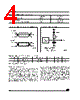
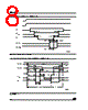
4 / 13 page  M27V322 4/13 Table 5. AC Measurement Conditions High Speed Standard Input Rise and Fall Times ≤ 10ns ≤ 20ns Input Pulse Voltages 0 to 3V 0.4V to 2.4V Input and Output Timing Ref. Voltages 1.5V 0.8V and 2V Figure 3. AC Testing Input Output Waveform AI01822 3V High Speed 0V 1.5V 2.4V Standard 0.4V 2.0V 0.8V Figure 4. AC Testing Load Circuit AI01823B 1.3V OUT CL CL = 30pF for High Speed CL = 100pF for Standard CL includes JIG capacitance 3.3k Ω 1N914 DEVICE UNDER TEST Table 6. Capacitance (1) (TA = 25 °C, f = 1 MHz) Note: 1. Sampled only, not 100% tested. Symbol Parameter Test Condition Min Max Unit CIN Input Capacitance VIN = 0V 10 pF COUT Output Capacitance VOUT = 0V 12 pF put control and by properly selected decoupling capacitors. It is recommended that a 0.1µF ceram- ic capacitor is used on every device between VCC and VSS. This should be a high frequency type of low inherent inductance and should be placed as close as possible to the device. In addition, a 4.7µF electrolytic capacitor should be used be- tween VCC and VSS for every eight devices. This capacitor should be mounted near the power sup- ply connection point. The purpose of this capacitor is to overcome the voltage drop caused by the in- ductive effects of PCB traces. System Considerations The power switching characteristics of Advanced CMOS EPROMs require careful decoupling of the supplies to the devices. The supply current ICC has three segments of importance to the system designer: the standby current, the active current and the transient peaks that are produced by the falling and rising edges of E. The magnitude of the transient current peaks is dependent on the ca- pacitive and inductive loading of the device out- puts. The associated transient voltage peaks can be suppressed by complying with the two line out- |
|
|
Lien URL |
| ALLDATASHEET vous a-t-il été utile ? [ DONATE ] |
À propos de Alldatasheet | Publicité | Contactez-nous | Politique de confidentialité | Lien vers la fiche technique | Echange de liens | Fabricants All Rights Reserved©Alldatasheet.com |
| Russian : Alldatasheetru.com | Korean : Alldatasheet.co.kr | Spanish : Alldatasheet.es | French : Alldatasheet.fr | Italian : Alldatasheetit.com Portuguese : Alldatasheetpt.com | Polish : Alldatasheet.pl | Vietnamese : Alldatasheet.vn Indian : Alldatasheet.in | Mexican : Alldatasheet.com.mx | British : Alldatasheet.co.uk | New Zealand : Alldatasheet.co.nz |
|
Family Site : ic2ic.com |
icmetro.com |
 French ▼
 English
 Chinese
 German
 Japanese
 Russian
 Korean
 Spanish
 French
 Italian
 Portuguese
 Polish
 Vietnamese
 Indian
 Mexican
 British
 New Zealand