|
Moteur de recherche de fiches techniques de composants électroniques |
|
|
Moteur de recherche de fiches techniques de composants électroniques |
|
G914X Fiches technique(PDF) 8 Page - Global Mixed-mode Technology Inc |
|
|
|||||||||||||||||||||||||||||
G914X Fiches technique(HTML) 8 Page - Global Mixed-mode Technology Inc |
|
|
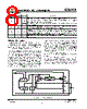
8 / 11 page  Ver: 1.8 Jul 24, 2007 TEL: 886-3-5788833 http://www.gmt.com.tw 8 G914X Global Mixed-mode Technology Inc. Pin Description PIN G914A~H G914Z NAME FUNCTION 1 1 IN Regulator Input. Supply voltage can range from +2.5V to +6.0V. Bypass with 1µF to GND 2 2 GND Ground. This pin also functions as a heatsink. Solder to large pads or the circuit board ground plane to maximize thermal dissipation. 3 3 SHDN Active-Low Shutdown Input. A logic low reduces the supply current to less than 1µA. Connect to IN for normal operation. 4 --- BYP This is a reference bypass pin. It should connect external 10nF capacitor to GND to reduce output noise. Bypass capacitor must be no less than 1nF. (CBYP≥ 1nF) --- 4 SET Feedback Input for Setting the Output Voltage. Connect to GND to set the output voltage to the preset output voltage. Connect to an external resistor divider for adjustable-output op- eration. The adjustable output voltage, VOUT, is then given by the following equation: VOUT = 1.25 (1 + R1/R2), Reference to Typical Application Circuit in Page 1. 5 5 OUT Regulator Output. Sources up to 300mA. Bypass with a 4.7µF, <0.2 Ω typical ESR ca- pacitor to GND. Detailed Description The block diagram of the G914X is shown in Figure 1. It consists of an error amplifier, 1.25V bandgap refer- ence, PMOS output transistor, internal feedback volt- age divider, shutdown logic, over current protection circuit, and over temperature protection circuit. The internal feedback voltage divider’s central tap is connected to the non-inverting input of the error ampli- fier. The error amplifier compares non-inverting input with the 1.25V bandgap reference. If the feedback voltage is higher than 1.25V, the error amplifier’s out- put becomes higher so that the PMOS output transis- tor has a smaller gate-to-source voltage (VGS). This reduces the current carrying capability of the PMOS output transistor, as a result the output voltage de- creases until the feedback voltage is equal to 1.25V. Similarly, when the feedback voltage is less than 1.25V, the error amplifier causes the output PMOS to conduct more current to pull the feedback voltage up to 1.25V. Thus, through this feedback action, the error amplifier, output PMOS, and the voltage divider effec- tively form a unity-gain amplifier with the feedback voltage force to be the same as the 1.25V bandgap reference. The output voltage, VOUT, is then given by the following equation: VOUT = 1.25 (1 + R1/R2). (1) Alternatively, the relationship between R1 and R2 is given by: R1 = R2 (VOUT / 1.25 + 1). (2) For the output voltage versions of G914X, the output voltages are 2.7V for G914A, 2.8V for G914B, 3.0V for G914C, 3.3V for G914D, and 2.5V for G914E, 2.85V for G914F, 1.50V for G914G and 1.80V for G914H. Figure 1. Functional Diagram SHDN IN OUT SHUTDOWN LOGIC 1.25V Vref - ERROR AMP + OVER CURRENT PROTECT & DYNAMIC FEEDBACK GND R1 R2 OVER TEMP. PROTECT BYP C BYP SHDN IN OUT SHUTDOWN LOGIC 1.25V Vref - ERROR AMP + OVER CURRENT PROTECT & DYNAMIC FEEDBACK GND R1 R2 OVER TEMP. PROTECT BYP C BYP |
|
|
Lien URL |
| ALLDATASHEET vous a-t-il été utile ? [ DONATE ] |
À propos de Alldatasheet | Publicité | Contactez-nous | Politique de confidentialité | Lien vers la fiche technique | Echange de liens | Fabricants All Rights Reserved©Alldatasheet.com |
| Russian : Alldatasheetru.com | Korean : Alldatasheet.co.kr | Spanish : Alldatasheet.es | French : Alldatasheet.fr | Italian : Alldatasheetit.com Portuguese : Alldatasheetpt.com | Polish : Alldatasheet.pl | Vietnamese : Alldatasheet.vn Indian : Alldatasheet.in | Mexican : Alldatasheet.com.mx | British : Alldatasheet.co.uk | New Zealand : Alldatasheet.co.nz |
|
Family Site : ic2ic.com |
icmetro.com |
 French ▼
 English
 Chinese
 German
 Japanese
 Russian
 Korean
 Spanish
 French
 Italian
 Portuguese
 Polish
 Vietnamese
 Indian
 Mexican
 British
 New Zealand