|
Moteur de recherche de fiches techniques de composants électroniques |
|
|
Moteur de recherche de fiches techniques de composants électroniques |
|
TS339CD Fiches technique(PDF) 3 Page - Taiwan Semiconductor Company, Ltd |
|
|
|||||||||||||||||||||||||||||
TS339CD Fiches technique(HTML) 3 Page - Taiwan Semiconductor Company, Ltd |
|
|
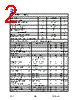
3 / 6 page  TS339 3-6 2003/12 rev. A Electrical Characteristics (Continues) Note 1. The maximum output current may be as high as 20mA, independent of the magnitude of VCC Output short circuits to VCC can cause excessive heating and eventual destruction. Note 2. This magnitude of input current will only occur if the leads are driven more negative than ground or the negative supply voltage. This is due to the input PNP collector base junction become forward biased, acting as an input clamp diode. There is also a lateral PNP parasitic transistor action which can cause the output voltage of the comparators to go to the VCC voltage level (or ground if overdrive is large) during the time that an input is driven negative. This will not destroy the device when limited to the max rating and normal output states will recover when the inputs become ≥ground or negative supply. Note 3. At the output switch point, VO=1.4Vdc, RS ≤100Ω, 5.0Vdc≤ VCC ≤30Vdc, with the inputs over the full common-mode range (0Vdc to VCC -1.5Vdc). Note 4. The bias current flows out of the inputs due to the PNP input stage. This current is virtually constant, independent of the output state. Note 5. The response time specified is for a 100mV input step with 5mV overdrive For larger signals, 300ns is typical. Note 6. Positive excursions of input voltage may exceed the power supply level. As long as one of the inputs remain within the common-mode range, the comparator will provide the proper output state. Note 7. The comparator will inhibit proper output state if one of the inputs is become greater than VCC, the other input must remain within the common mode range. The low input state must not be less than -0.3volts of ground of minus supply. |
|
|
Lien URL |
| ALLDATASHEET vous a-t-il été utile ? [ DONATE ] |
À propos de Alldatasheet | Publicité | Contactez-nous | Politique de confidentialité | Lien vers la fiche technique | Echange de liens | Fabricants All Rights Reserved©Alldatasheet.com |
| Russian : Alldatasheetru.com | Korean : Alldatasheet.co.kr | Spanish : Alldatasheet.es | French : Alldatasheet.fr | Italian : Alldatasheetit.com Portuguese : Alldatasheetpt.com | Polish : Alldatasheet.pl | Vietnamese : Alldatasheet.vn Indian : Alldatasheet.in | Mexican : Alldatasheet.com.mx | British : Alldatasheet.co.uk | New Zealand : Alldatasheet.co.nz |
|
Family Site : ic2ic.com |
icmetro.com |
 French ▼
 English
 Chinese
 German
 Japanese
 Russian
 Korean
 Spanish
 French
 Italian
 Portuguese
 Polish
 Vietnamese
 Indian
 Mexican
 British
 New Zealand