|
Moteur de recherche de fiches techniques de composants électroniques |
|
|
Moteur de recherche de fiches techniques de composants électroniques |
|
TC1304-AO2EUNTR Fiches technique(PDF) 19 Page - Microchip Technology |
|
|
|||||||||||||||||||||||||||||
TC1304-AO2EUNTR Fiches technique(HTML) 19 Page - Microchip Technology |
|
|
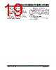
19 / 36 page  © 2005 Microchip Technology Inc. DS21949B-page 19 TC1303A/TC1303B/TC1303C/TC1304 3.9 Buck Regulator Input Voltage Pin (VIN1) VIN1 is the buck regulator power input supply pin. Connect a variable input voltage source to VIN1. Connect VIN1 and VIN2 together with board traces as short as possible. 3.10 Buck Inductor Output Pin (LX) Connect LX directly to the buck inductor. This pin carries large signal-level current; all connections should be made as short as possible. 3.11 Power Ground Pin (PGND) Connect all large-signal level ground returns to PGND. These large-signal, level ground traces should have a small loop area and length to prevent coupling of switching noise to sensitive traces. Please see the physical layout information supplied in Section 5.0 “Application Circuits/Issues” for grounding recommendations. 3.12 Exposed Pad (EP) For the DFN package, connect the EP to AGND, with vias into the AGND plane. |
|
Lien URL |
| ALLDATASHEET vous a-t-il été utile ? [ DONATE ] |
À propos de Alldatasheet | Publicité | Contactez-nous | Politique de confidentialité | Lien vers la fiche technique | Echange de liens | Fabricants All Rights Reserved©Alldatasheet.com |
| Russian : Alldatasheetru.com | Korean : Alldatasheet.co.kr | Spanish : Alldatasheet.es | French : Alldatasheet.fr | Italian : Alldatasheetit.com Portuguese : Alldatasheetpt.com | Polish : Alldatasheet.pl | Vietnamese : Alldatasheet.vn Indian : Alldatasheet.in | Mexican : Alldatasheet.com.mx | British : Alldatasheet.co.uk | New Zealand : Alldatasheet.co.nz |
|
Family Site : ic2ic.com |
icmetro.com |
 French ▼
 English
 Chinese
 German
 Japanese
 Russian
 Korean
 Spanish
 French
 Italian
 Portuguese
 Polish
 Vietnamese
 Indian
 Mexican
 British
 New Zealand