|
Moteur de recherche de fiches techniques de composants électroniques |
|
|
Moteur de recherche de fiches techniques de composants électroniques |
|
AD633JRZ-R7 Fiches technique(PDF) 8 Page - Analog Devices |
|
|
|||||||||||||||||||||||||||||
AD633JRZ-R7 Fiches technique(HTML) 8 Page - Analog Devices |
|
|
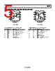
8 / 20 page  AD633 Data Sheet FUNCTIONAL DESCRIPTION The AD633 is a low cost multiplier comprising a translinear core, a buried Zener reference, and a unity-gain connected output amplifier with an accessible summing node. Figure 1 shows the functional block diagram. The differential X and Y inputs are converted to differential currents by voltage-to-current converters. The product of these currents is generated by the multiplying core. A buried Zener reference provides an overall scale factor of 10 V. The sum of (X × Y)/10 + Z is then applied to the output amplifier. The amplifier summing Node Z allows the user to add two or more multiplier outputs, convert the output voltage to a current, and configure various analog computational functions. Inspection of the block diagram shows the overall transfer function is ( )( ) Z Y2 Y1 X2 X1 W + − − = V 10 (1) ERROR SOURCES Multiplier errors consist primarily of input and output offsets, scale factor error, and nonlinearity in the multiplying core. The input and output offsets can be eliminated by using the optional trim of Figure 11. This scheme reduces the net error to scale factor errors (gain error) and an irreducible nonlinearity component in the multiplying core. The X and Y nonlinearities are typically 0.4% and 0.1% of full scale, respectively. Scale factor error is typically 0.25% of full scale. The high impedance Z input should always reference the ground point of the driven system, particularly if it is remote. Likewise, the differential X and Y inputs should reference their respective grounds to realize the full accuracy of the AD633. ±50mV TO APPROPRIATE INPUT TERMINAL (FOR EXAMPLE, X2, Y2, Z) 50kΩ 1kΩ 300kΩ +VS –VS Figure 11. Optional Offset Trim Configuration Rev. K | Page 8 of 20 |
|
|
Lien URL |
| ALLDATASHEET vous a-t-il été utile ? [ DONATE ] |
À propos de Alldatasheet | Publicité | Contactez-nous | Politique de confidentialité | Lien vers la fiche technique | Echange de liens | Fabricants All Rights Reserved©Alldatasheet.com |
| Russian : Alldatasheetru.com | Korean : Alldatasheet.co.kr | Spanish : Alldatasheet.es | French : Alldatasheet.fr | Italian : Alldatasheetit.com Portuguese : Alldatasheetpt.com | Polish : Alldatasheet.pl | Vietnamese : Alldatasheet.vn Indian : Alldatasheet.in | Mexican : Alldatasheet.com.mx | British : Alldatasheet.co.uk | New Zealand : Alldatasheet.co.nz |
|
Family Site : ic2ic.com |
icmetro.com |
 French ▼
 English
 Chinese
 German
 Japanese
 Russian
 Korean
 Spanish
 French
 Italian
 Portuguese
 Polish
 Vietnamese
 Indian
 Mexican
 British
 New Zealand