|
Moteur de recherche de fiches techniques de composants électroniques |
|
|
Moteur de recherche de fiches techniques de composants électroniques |
|
AOZ9510QI Fiches technique(PDF) 10 Page - Alpha & Omega Semiconductors |
|
|
|||||||||||||||||||||||||||||
AOZ9510QI Fiches technique(HTML) 10 Page - Alpha & Omega Semiconductors |
|
|
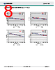
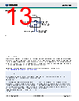
10 / 13 page  Rev. 1.3 September 2022 www.aosmd.com Page 10 of 13 AOZ9510QI Layout Considerations Several layout tips are listed below for the best electric and thermal performance. 1. The VIN pins and pad are connected to internal high side switch drain. They are also low resistance thermal conduction path. Connected a large copper plane to VIN pins to help thermal dissipation. 2. Input capacitors should be connected to the VIN pins and the PGND pins as close as possible to reduce the switching spikes. 3. The VOUT pins and pad are connected to internal low side switch drain. They are low resistance thermal conduction path and most noisy switching node. Connected a large copper plane to VOUT pins to help thermal dissipation. 4. Decoupling capacitor CVCC should be connected to VCC and AGND as close as possible. 5. Bootstrap capacitor CB should be connected to VB and VOUT as close as possible. 6. A ground plane is preferred; PGND and AGND must be connected to the ground plane through vias. 7. Keep sensitive signal traces such as feedback trace and digital signals far away from the VOUT pins. Figure 13. Layout Placement 1 VIN VOUT 2 3 4 5 6 VOUT DVS2 DVS1 NC HIN LIN VTP PGND 16 15 13 12 14 17 |
|
|
Lien URL |
| ALLDATASHEET vous a-t-il été utile ? [ DONATE ] |
À propos de Alldatasheet | Publicité | Contactez-nous | Politique de confidentialité | Lien vers la fiche technique | Echange de liens | Fabricants All Rights Reserved©Alldatasheet.com |
| Russian : Alldatasheetru.com | Korean : Alldatasheet.co.kr | Spanish : Alldatasheet.es | French : Alldatasheet.fr | Italian : Alldatasheetit.com Portuguese : Alldatasheetpt.com | Polish : Alldatasheet.pl | Vietnamese : Alldatasheet.vn Indian : Alldatasheet.in | Mexican : Alldatasheet.com.mx | British : Alldatasheet.co.uk | New Zealand : Alldatasheet.co.nz |
|
Family Site : ic2ic.com |
icmetro.com |
 French ▼
 English
 Chinese
 German
 Japanese
 Russian
 Korean
 Spanish
 French
 Italian
 Portuguese
 Polish
 Vietnamese
 Indian
 Mexican
 British
 New Zealand