|
Moteur de recherche de fiches techniques de composants électroniques |
|
|
Moteur de recherche de fiches techniques de composants électroniques |
|
L99MOD51XP Fiches technique(PDF) 8 Page - STMicroelectronics |
|
|
|||||||||||||||||||||||||||||
L99MOD51XP Fiches technique(HTML) 8 Page - STMicroelectronics |
|
|
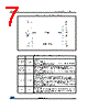
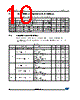
8 / 33 page  Block diagram and pin description L99MOD51XP 8/33 DS12667 Rev 6 9 CM/PWM Current monitor output/PWM input. Depending on the selected multiplexer bits (bit 9, 10, 11) of Input Data Register this output sources an image of the instant current through the corresponding high side driver with a ratio of 1/10.000. This pin is bidirectional. The microcontroller can overwrite the current monitor signal to provide a PWM input for all outputs. 10 CSN Chip select not input. This input is low active and requires CMOS logic levels. The serial data transfer between L99MOD51XP and micro controller is enabled by pulling the input CSN to low level. 11 DO Serial data output. The diagnosis data is available via the SPI and this tristate-output. The output will remain in tristate, if the chip is not selected by the input CSN (CSN = high). 12 VCC Logic supply voltage. For this input a ceramic capacitor as close as possible to GND is recommended. 13 CLK Serial clock input. This input controls the internal shift register of the SPI and requires CMOS logic levels. 16, 17 OUT2 Half-bridge output 2 (see OUT1 - pin 3, 4). Note: for the capability of driving the full current at the outputs all pins of OUT2 must be externally connected. 20, 21 OUT3 Half-bridge output 3 (see OUT1 - pin 3, 4). Note: for the capability of driving the full current at the outputs all pins of OUT3 must be externally connected. 26 CP Charge Pump Output. This output is provided to drive the gate of an external n-channel power MOS used for reverse polarity protection (see Figure 1). 27 EN Enable input. If Enable input is forced to GND the device will enter in Standby-Mode. The outputs will be switched off and all registers will be cleared 33, 35 OUT4, OUT5 High side driver output 4, 5. The output is built by a high side switch and is intended for resistive loads, hence the internal reverse diode from GND to the output is missing. For ESD reason a diode to GND is present but the energy which can be dissipated is limited. The high side driver is a power DMOS transistor with an internal reverse diode from the output to VS (bulk- drain-diode). The output is over-current and open-load protected. Table 2. Pin definitions and functions (continued) Pin Symbol Function |
|
Lien URL |
| ALLDATASHEET vous a-t-il été utile ? [ DONATE ] |
À propos de Alldatasheet | Publicité | Contactez-nous | Politique de confidentialité | Lien vers la fiche technique | Echange de liens | Fabricants All Rights Reserved©Alldatasheet.com |
| Russian : Alldatasheetru.com | Korean : Alldatasheet.co.kr | Spanish : Alldatasheet.es | French : Alldatasheet.fr | Italian : Alldatasheetit.com Portuguese : Alldatasheetpt.com | Polish : Alldatasheet.pl | Vietnamese : Alldatasheet.vn Indian : Alldatasheet.in | Mexican : Alldatasheet.com.mx | British : Alldatasheet.co.uk | New Zealand : Alldatasheet.co.nz |
|
Family Site : ic2ic.com |
icmetro.com |
 French ▼
 English
 Chinese
 German
 Japanese
 Russian
 Korean
 Spanish
 French
 Italian
 Portuguese
 Polish
 Vietnamese
 Indian
 Mexican
 British
 New Zealand