|
Moteur de recherche de fiches techniques de composants électroniques |
|
|
Moteur de recherche de fiches techniques de composants électroniques |
|
AL1666 Fiches technique(PDF) 10 Page - Diodes Incorporated |
|
|
|||||||||||||||||||||||||||||
AL1666 Fiches technique(HTML) 10 Page - Diodes Incorporated |
|
|
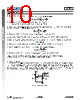
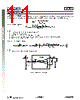
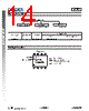
10 / 16 page  AL1666 Document number: DS42417 Rev. 1 - 2 10 of 16 www.diodes.com December 2019 © Diodes Incorporated AL1666 Application Information (continued) Output Constant-Current Control According to the definition of mean output current, the mean output current can be obtained as below. dt t t I I SW ONS SP MEAN O 0 _ 2 1 1 Where IO_MEAN is the mean output current; ISP is secondary peak current of transformer; tONS is discharge time of secondary side of transformer; tSW is the switch period. According to the principle of AL1666 close loop control, the voltage of RCS will be sampled when switch is turned off and the value will be held until discharge time tONS is over. It can be described by following formula: VREF= 1 π ∫ IP π 0 ∙RCS∙ tONS tSW dt Where IP is primary peak current of transformer; RCS is current sense resister which is shown as Figure 1. tONS is discharge time of secondary side of transformer; tSW is the switch period. VREF is internal reference voltage that is equal to 0.4V. The peak current at secondary side has following relationship with primary side peak current, if the effect of the leakage inductor is neglected. SP PS P I N I Where NPS is the turns ratio of Flyback transformer (NPS=1 for Buck-boost); IP is the primary peak current of the transformer. According to these above formulas, the mean output current can be induced finally by below expressions. _ 2 PS REF O MEAN CS NV I R Where IO_MEAN is the mean output current; RCS is current sense resister which is shown as Figure 1 and Figure 2; VREF is internal reference voltage that is equal to 0.4V; NPS is the turns ratio of Flyback transformer (NPS=1 for Buck-boost); Therefore, the constant output current control can be realized with appropriate parameter design. PF and THD Compensation Circuit In typical application, the AL1666 can provide PF>0.9 and THD <20%. It can improve PF>0.95 and THD<10% by adding the below compensation circuit. VBUS is connected to bus line which is after rectifier bridge. COMP pin voltage will add an offset that almost follows with bus line voltage in the circuit. Due to COMP voltage controls switch-on time, thus phase difference between input voltage and input current will be reduced that can optimize PF and THD. In the circuit, range of resister value R12 is from 800k Ω to 1.5MΩ, range of resistor value R13 is from 500Ω resistor to 5.1kΩ. Range of capacitance C11 is 1 F to 2F. PF and THD can be improved by fine tuning these components. COMP CCOMP RCOMP VBUS C11 R12 R13 Figure 3. PF and THD Optimization Circuit |
|
|
Lien URL |
| ALLDATASHEET vous a-t-il été utile ? [ DONATE ] |
À propos de Alldatasheet | Publicité | Contactez-nous | Politique de confidentialité | Lien vers la fiche technique | Echange de liens | Fabricants All Rights Reserved©Alldatasheet.com |
| Russian : Alldatasheetru.com | Korean : Alldatasheet.co.kr | Spanish : Alldatasheet.es | French : Alldatasheet.fr | Italian : Alldatasheetit.com Portuguese : Alldatasheetpt.com | Polish : Alldatasheet.pl | Vietnamese : Alldatasheet.vn Indian : Alldatasheet.in | Mexican : Alldatasheet.com.mx | British : Alldatasheet.co.uk | New Zealand : Alldatasheet.co.nz |
|
Family Site : ic2ic.com |
icmetro.com |
 French ▼
 English
 Chinese
 German
 Japanese
 Russian
 Korean
 Spanish
 French
 Italian
 Portuguese
 Polish
 Vietnamese
 Indian
 Mexican
 British
 New Zealand