|
Moteur de recherche de fiches techniques de composants électroniques |
|
|
Moteur de recherche de fiches techniques de composants électroniques |
|
IS25LP032D-RGLA3 Fiches technique(PDF) 10 Page - Integrated Silicon Solution, Inc |
|
|
|||||||||||||||||||||||||||||
IS25LP032D-RGLA3 Fiches technique(HTML) 10 Page - Integrated Silicon Solution, Inc |
|
|
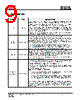
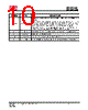
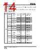
10 / 118 page  IS25LP032D IS25WP032D Integrated Silicon Solution, Inc.- www.issi.com 10 Rev. A12 08/04/2020 SYMBOL TYPE DESCRIPTION RESET# INPUT/OUTPUT RESET#: This dedicated RESET# is available in 16-pin SOIC and 24-ball BGA packages. The RESET# pin is a hardware RESET signal. When RESET# is driven HIGH, the memory is in the normal operating mode. When RESET# is driven LOW, the memory enters reset mode and output is High-Z. If RESET# is driven LOW while an internal WRITE, PROGRAM, or ERASE operation is in progress, data may be lost. Dedicated RESET# function can be Disabled when bit 0 of Function Register = 1. It has an internal pull-up resistor and may be left floating if not used. SCK INPUT Serial Data Clock: Synchronized Clock for input and output timing operations. Vcc POWER Power: Device Core Power Supply GND GROUND Ground: Connect to ground when referenced to Vcc NC Unused NC: Pins labeled “NC” stand for “No Connect” and should be left uncommitted. |
|
Lien URL |
| ALLDATASHEET vous a-t-il été utile ? [ DONATE ] |
À propos de Alldatasheet | Publicité | Contactez-nous | Politique de confidentialité | Lien vers la fiche technique | Echange de liens | Fabricants All Rights Reserved©Alldatasheet.com |
| Russian : Alldatasheetru.com | Korean : Alldatasheet.co.kr | Spanish : Alldatasheet.es | French : Alldatasheet.fr | Italian : Alldatasheetit.com Portuguese : Alldatasheetpt.com | Polish : Alldatasheet.pl | Vietnamese : Alldatasheet.vn Indian : Alldatasheet.in | Mexican : Alldatasheet.com.mx | British : Alldatasheet.co.uk | New Zealand : Alldatasheet.co.nz |
|
Family Site : ic2ic.com |
icmetro.com |
 French ▼
 English
 Chinese
 German
 Japanese
 Russian
 Korean
 Spanish
 French
 Italian
 Portuguese
 Polish
 Vietnamese
 Indian
 Mexican
 British
 New Zealand