|
Moteur de recherche de fiches techniques de composants électroniques |
|
|
Moteur de recherche de fiches techniques de composants électroniques |
|
IS25LP032D-RGLA3:P Fiches technique(PDF) 86 Page - Integrated Silicon Solution, Inc |
|
|
|||||||||||||||||||||||||||||
IS25LP032D-RGLA3:P Fiches technique(HTML) 86 Page - Integrated Silicon Solution, Inc |
|
|
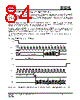
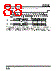
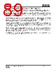
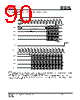
86 / 118 page  IS25LP032D IS25WP032D Integrated Silicon Solution, Inc.- www.issi.com 86 Rev. A12 08/04/2020 8.40 FAST READ DUAL IO DTR MODE OPERATION (FRDDTR, BDh) The FRDDTR instruction enables Double Transfer Rate throughput on dual I/O of the device in read mode. The address (interleave on dual I/O pins) is latched on both rising and falling edge of SCK, and the data (interleave on dual I/O pins) shift out on both rising and falling edge of SCK at a maximum frequency. The 4-bit address can be latched-in at one clock, and 4-bit data can be read out at one clock, which means two bits at the rising edge of clock, the other two bits at the falling edge of clock. The first address byte can be at any location. The address is automatically increased to the next higher address after each byte of data is shifted out, so the whole memory can be read out with a single FRDDTR instruction. The address counter rolls over to 0 when the highest address is reached. Once writing FRDDTR instruction, the following address/dummy/data out will perform as 4-bit instead of previous 1-bit. The sequence of issuing FRDDTR instruction is: CE# goes low Sending FRDDTR instruction (1-bit per clock) 24-bit address interleave on IO1 & IO0 (4-bit per clock) 4 dummy clocks (configurable, default is 4 clocks) on IO1 & IO0 Data out interleave on IO1 & IO0 (4-bit per clock) End FRDDTR operation via pulling CE# high at any time during data out (Please refer to Figure 8.65 for 2 x I/O Double Transfer Rate Read Mode Timing Waveform). If AXh ( where X is don’t care) is input for the mode bits during dummy cycles, the device will enter AX read operation mode which enables subsequent FRDDTR execution skips command code. It saves cycles as described in Figure 8.66. When the code is different from AXh, the device exits the AX read operation. After finishing the read operation, device becomes ready to receive a new command. If the FRDDTR instruction is issued while a Program/Erase/Write Status Register cycle is in progress (WIP=1), the instruction will be rejected without any effect on the current cycle. |
|
Lien URL |
| ALLDATASHEET vous a-t-il été utile ? [ DONATE ] |
À propos de Alldatasheet | Publicité | Contactez-nous | Politique de confidentialité | Lien vers la fiche technique | Echange de liens | Fabricants All Rights Reserved©Alldatasheet.com |
| Russian : Alldatasheetru.com | Korean : Alldatasheet.co.kr | Spanish : Alldatasheet.es | French : Alldatasheet.fr | Italian : Alldatasheetit.com Portuguese : Alldatasheetpt.com | Polish : Alldatasheet.pl | Vietnamese : Alldatasheet.vn Indian : Alldatasheet.in | Mexican : Alldatasheet.com.mx | British : Alldatasheet.co.uk | New Zealand : Alldatasheet.co.nz |
|
Family Site : ic2ic.com |
icmetro.com |
 French ▼
 English
 Chinese
 German
 Japanese
 Russian
 Korean
 Spanish
 French
 Italian
 Portuguese
 Polish
 Vietnamese
 Indian
 Mexican
 British
 New Zealand