|
Moteur de recherche de fiches techniques de composants électroniques |
|
|
Moteur de recherche de fiches techniques de composants électroniques |
|
INMP510ACEZ-R7 Fiches technique(PDF) 10 Page - TDK Electronics |
|
|
|||||||||||||||||||||||||||||
INMP510ACEZ-R7 Fiches technique(HTML) 10 Page - TDK Electronics |
|
|
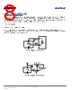
10 / 13 page  INMP510 PCB DESIGN AND LAND PATTERN LAYOUT The recommended PCB land pattern for the INMP504 should be laid out to a 1:1 ratio to the solder pads on the microphone package, as shown in Figure 8. Take care to avoid applying solder paste to the sound hole in the PCB. A suggested solder paste stencil pattern layout is shown in Figure 9. The diameter of the sound hole in the PCB should be larger than the diameter of the sound port of the microphone. A minimum diameter of 0.5 mm is recommended. Dimensions shown in millimeters Figure 11. PCB Land Pattern Layout Dimensions shown in millimeters Figure 12. Suggested Solder Paste Stencil Pattern Layout Ø1.55 Ø0.95 1.52 0.90 1.90 1.22 0.68 0.61 0.61 1.22 2× 0.8 × 0.6 0.2 × 45 TYP 1.52mm 1.55/1.05 DIA. 0.225 CUT WIDTH (2×) Page 10 of 13 Document Number: DS-INMP510-00 Revision: 1.0. |
|
|
Lien URL |
| ALLDATASHEET vous a-t-il été utile ? [ DONATE ] |
À propos de Alldatasheet | Publicité | Contactez-nous | Politique de confidentialité | Lien vers la fiche technique | Echange de liens | Fabricants All Rights Reserved©Alldatasheet.com |
| Russian : Alldatasheetru.com | Korean : Alldatasheet.co.kr | Spanish : Alldatasheet.es | French : Alldatasheet.fr | Italian : Alldatasheetit.com Portuguese : Alldatasheetpt.com | Polish : Alldatasheet.pl | Vietnamese : Alldatasheet.vn Indian : Alldatasheet.in | Mexican : Alldatasheet.com.mx | British : Alldatasheet.co.uk | New Zealand : Alldatasheet.co.nz |
|
Family Site : ic2ic.com |
icmetro.com |
 French ▼
 English
 Chinese
 German
 Japanese
 Russian
 Korean
 Spanish
 French
 Italian
 Portuguese
 Polish
 Vietnamese
 Indian
 Mexican
 British
 New Zealand