 |
Moteur de recherche de fiches techniques de composants électroniques |
|
|
Moteur de recherche de fiches techniques de composants électroniques |
|
The question interval is too short.
Please try again in a few seconds.

Hello, Please ask a question about CY7C1327G_13 Datasheet
# Example questions:
➢ What happens to the sram's output drivers when a write cycle is detected, regardless of the state of the output enable (oe) signal?
➢ What determines whether the cy7c1327g will use a linear or interleaved burst sequence?
➢ What is guaranteed while the device is in this mode?
| Part No. | CY7C1327G_13 |
| Manufacturer | CYPRESS |
| Size | 779 Kbytes |
| Pages | 23 pages |
| Description | 4-Mbit (256 K x 18) Pipelined Sync SRAM |

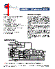
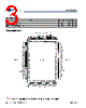


1. Overview & Purpose
️· What it is: A synchronous static RAM (SRAM) device.
️· Purpose: Designed primarily as a secondary cache memory for computer systems, suitable for both linear and interleaved burst sequences. Specifically mentions support for Intel Pentium and i486 processors (for interleaved bursts) and processors that utilize linear burst sequences.
️· Key Features: Synchronous operation, self-timed write circuitry, multiple chip select lines, byte write capability, sleep mode for power conservation.
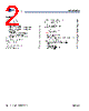
2. Key Signals and Their Functions
️· Clock (tCYC): The clock signal controls the synchronous operation of the device.
️· CE1, CE2, CE3 (Chip Selects): Synchronous chip select lines for bank selection.
️· ADSP (Address Strobe Processor): Initiates memory access.
️· ADSC (Address Strobe Controller): Initiates memory access, used as an alternative to ADSP.
️· GW (Global Write Enable): Overrides byte write inputs and performs a global write to all bytes.
️· BWE (Byte Write Enable): Enables byte write operations.
️· BW[A:B] (Byte Write Select): Selects specific bytes for byte write operations.
️· ADV (Address Advancement): Automatically increments the address for burst operations.
️· MODE (Burst Mode Select): Selects between linear and interleaved burst modes.
️· OE (Output Enable): Controls the output drivers. Must be high before data is presented to the DQ inputs.
️· DQ (Data Input/Output): Data bus lines.
️· ZZ (Sleep Mode Enable): Places the device into a low-power sleep mode.
3. Burst Modes
️· Linear Burst Mode (MODE = GND): Sequential address access. See the "Linear Burst Address Table" for address sequence.
️· Interleaved Burst Mode (MODE = Floating or VDD): Optimized for Intel processors. See the "Interleaved Burst Address Table" for address sequence.
4. Write Operations
️· Single Write (ADSP): Requires two clock cycles.
️· Single Write (ADSC): Completed in one clock cycle. A faster option.
️· Byte Write: Allows selective writing to individual bytes within a word.
️· Global Write: Writes to all bytes simultaneously (overrides byte enables).
5. Sleep Mode
️· Activation: Places the device in a low-power state.
️· Requirements: Requires two clock cycles to enter and exit.
️· Considerations: Accesses in progress are not valid and must be discarded before entering sleep mode. Certain signals must remain inactive during entry and exit.
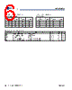
️· Electrical Characteristics: Some key electrical characteristics related to power consumption in sleep mode are given (IDDZZ, tZZS, tZZREC, tZZI, tRZZI).
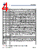
6. Electrical Characteristics and Timings (Important for Design)
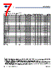
️· The document includes tables specifying electrical characteristics related to sleep mode. There are other, unspecified, electrical characteristics relating to general operation.
️· It gives timings (e.g., the two-cycle requirement for entering and exiting sleep mode) that are critical for system design.
Key Takeaways
️· This is a robust and versatile SRAM designed for cache memory applications.
️· The burst modes, byte write capability, and sleep mode offer flexibility and performance benefits.
️· Careful attention to the signal timings and electrical characteristics is necessary for proper system integration.
1. Overview & Purpose
️· What it is: A synchronous static RAM (SRAM) device.
️· Purpose: Designed primarily as a secondary cache memory for computer systems, suitable for both linear and interleaved burst sequences. Specifically mentions support for Intel Pentium and i486 processors (for interleaved bursts) and processors that utilize linear burst sequences.
️· Key Features: Synchronous operation, self-timed write circuitry, multiple chip select lines, byte write capability, sleep mode for power conservation.
2. Key Signals and Their Functions
️· Clock (tCYC): The clock signal controls the synchronous operation of the device.
️· CE1, CE2, CE3 (Chip Selects): Synchronous chip select lines for bank selection.
️· ADSP (Address Strobe Processor): Initiates memory access.
️· ADSC (Address Strobe Controller): Initiates memory access, used as an alternative to ADSP.
️· GW (Global Write Enable): Overrides byte write inputs and performs a global write to all bytes.
️· BWE (Byte Write Enable): Enables byte write operations.
️· BW[A:B] (Byte Write Select): Selects specific bytes for byte write operations.
️· ADV (Address Advancement): Automatically increments the address for burst operations.
️· MODE (Burst Mode Select): Selects between linear and interleaved burst modes.
️· OE (Output Enable): Controls the output drivers. Must be high before data is presented to the DQ inputs.
️· DQ (Data Input/Output): Data bus lines.
️· ZZ (Sleep Mode Enable): Places the device into a low-power sleep mode.
3. Burst Modes
️· Linear Burst Mode (MODE = GND): Sequential address access. See the "Linear Burst Address Table" for address sequence.
️· Interleaved Burst Mode (MODE = Floating or VDD): Optimized for Intel processors. See the "Interleaved Burst Address Table" for address sequence.
4. Write Operations
️· Single Write (ADSP): Requires two clock cycles.
️· Single Write (ADSC): Completed in one clock cycle. A faster option.
️· Byte Write: Allows selective writing to individual bytes within a word.
️· Global Write: Writes to all bytes simultaneously (overrides byte enables).
5. Sleep Mode
️· Activation: Places the device in a low-power state.
️· Requirements: Requires two clock cycles to enter and exit.
️· Considerations: Accesses in progress are not valid and must be discarded before entering sleep mode. Certain signals must remain inactive during entry and exit.
️· Electrical Characteristics: Some key electrical characteristics related to power consumption in sleep mode are given (IDDZZ, tZZS, tZZREC, tZZI, tRZZI).
6. Electrical Characteristics and Timings (Important for Design)
️· The document includes tables specifying electrical characteristics related to sleep mode. There are other, unspecified, electrical characteristics relating to general operation.
️· It gives timings (e.g., the two-cycle requirement for entering and exiting sleep mode) that are critical for system design.
Key Takeaways
️· This is a robust and versatile SRAM designed for cache memory applications.
️· The burst modes, byte write capability, and sleep mode offer flexibility and performance benefits.
️· Careful attention to the signal timings and electrical characteristics is necessary for proper system integration.
| Part No. | CY7C1327G_13 |
| Manufacturer | CYPRESS |
| Size | 779 Kbytes |
| Pages | 23 pages |
| Description | 4-Mbit (256 K x 18) Pipelined Sync SRAM |
| ALLDATASHEET vous a-t-il été utile ? [ DONATE ] |
À propos de Alldatasheet | Publicité | Contactez-nous | Politique de confidentialité | Lien vers la fiche technique | Echange de liens | Fabricants All Rights Reserved©Alldatasheet.com |
| Russian : Alldatasheetru.com | Korean : Alldatasheet.co.kr | Spanish : Alldatasheet.es | French : Alldatasheet.fr | Italian : Alldatasheetit.com Portuguese : Alldatasheetpt.com | Polish : Alldatasheet.pl | Vietnamese : Alldatasheet.vn Indian : Alldatasheet.in | Mexican : Alldatasheet.com.mx | British : Alldatasheet.co.uk | New Zealand : Alldatasheet.co.nz |
|
Family Site : ic2ic.com |
icmetro.com |
 French ▼
  English
 Chinese
 German
 Japanese
 Russian
 Korean
 Spanish
 Italian
 Portuguese
 Polish
 Vietnamese
 Indian
 Mexican
 British
 New Zealand