 |
Moteur de recherche de fiches techniques de composants électroniques |
|
|
Moteur de recherche de fiches techniques de composants électroniques |
|
The question interval is too short.
Please try again in a few seconds.

Hello, Please ask a question about AM29F002BB-55JC Datasheet
# Example questions:
➢ What components are involved in the process of reading data from the memory array?
➢ Describe the function of the 'reset#' pin as indicated in the connection diagram and block diagram.
➢ What are the speed options available for the am29f002b, and what does the '-70' designation represent?
| Part No. | AM29F002BB-55JC |
| Manufacturer | AMD |
| Size | 796 Kbytes |
| Pages | 42 pages |
| Description | 2 Megabit (256 K x 8-Bit) CMOS 5.0 Volt-only Boot Sector Flash Memory |











1. Device Overview:
️· What: This document describes the Am29F002B and Am29F002NB, which are 2 Mbit (32K x 16) flash memory devices.
️· Flash Memory: They are non-volatile, meaning they retain data even when power is removed.
️· Key Difference: The Am29F002NB has a "NC" (Not Connected) on a pin, likely related to features or functionality that differ from the Am29F002B.
2. Speed Options & Product Selector Guide:
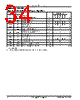
️· The devices are available in three speed options, denoted by suffixes:
- -55 (55ns access time)
- -70 (70ns access time)
- -90 (90ns access time)
️· The speed option determines the access times for CE# (Chip Enable) and OE# (Output Enable).
3. Connection Diagrams:
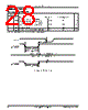
️· These diagrams show the pinout of the devices.
️· They highlight the functions of each pin (e.g., VCC, VSS, CE#, OE#, WE#, A0-A17, DQ0-DQ7, RESET#).
4. Block Diagram:
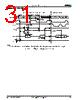
️· A visual representation of the internal architecture of the flash memory device.
️· Key components shown: Input/Output Buffers, X-Decoder, Y-Decoder, Chip Enable Logic, Erase Voltage Generator, PGM Voltage Generator, Timer, VCC Detector, Address Latch, Data Latch, Cell Matrix.
️· The block diagram helps understand how the device operates at a higher level.
5. Key Features/Functionality (Implied from the document):
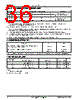
️· Erase and Program: The device can be erased and programmed using specific voltage levels (generated by the Erase Voltage Generator and PGM Voltage Generator).
️· VCC Detection: A VCC detector likely ensures proper operation within a defined voltage range.
️· Sectored Memory: The "Sector Switches" in the block diagram suggest that the memory is organized into sectors, which simplifies the erasure process.
In simpler terms:
This excerpt describes a flash memory chip with different speed options. It shows how the chip connects to other components and gives a basic understanding of how it works internally. The NB version has slight differences (the NC pin).
1. Device Overview:
️· What: This document describes the Am29F002B and Am29F002NB, which are 2 Mbit (32K x 16) flash memory devices.
️· Flash Memory: They are non-volatile, meaning they retain data even when power is removed.
️· Key Difference: The Am29F002NB has a "NC" (Not Connected) on a pin, likely related to features or functionality that differ from the Am29F002B.
2. Speed Options & Product Selector Guide:
️· The devices are available in three speed options, denoted by suffixes:
- -55 (55ns access time)
- -70 (70ns access time)
- -90 (90ns access time)
️· The speed option determines the access times for CE# (Chip Enable) and OE# (Output Enable).
3. Connection Diagrams:
️· These diagrams show the pinout of the devices.
️· They highlight the functions of each pin (e.g., VCC, VSS, CE#, OE#, WE#, A0-A17, DQ0-DQ7, RESET#).
4. Block Diagram:
️· A visual representation of the internal architecture of the flash memory device.
️· Key components shown: Input/Output Buffers, X-Decoder, Y-Decoder, Chip Enable Logic, Erase Voltage Generator, PGM Voltage Generator, Timer, VCC Detector, Address Latch, Data Latch, Cell Matrix.
️· The block diagram helps understand how the device operates at a higher level.
5. Key Features/Functionality (Implied from the document):
️· Erase and Program: The device can be erased and programmed using specific voltage levels (generated by the Erase Voltage Generator and PGM Voltage Generator).
️· VCC Detection: A VCC detector likely ensures proper operation within a defined voltage range.
️· Sectored Memory: The "Sector Switches" in the block diagram suggest that the memory is organized into sectors, which simplifies the erasure process.
In simpler terms:
This excerpt describes a flash memory chip with different speed options. It shows how the chip connects to other components and gives a basic understanding of how it works internally. The NB version has slight differences (the NC pin).
| Part No. | AM29F002BB-55JC |
| Manufacturer | AMD |
| Size | 796 Kbytes |
| Pages | 42 pages |
| Description | 2 Megabit (256 K x 8-Bit) CMOS 5.0 Volt-only Boot Sector Flash Memory |
| ALLDATASHEET vous a-t-il été utile ? [ DONATE ] |
À propos de Alldatasheet | Publicité | Contactez-nous | Politique de confidentialité | Lien vers la fiche technique | Echange de liens | Fabricants All Rights Reserved©Alldatasheet.com |
| Russian : Alldatasheetru.com | Korean : Alldatasheet.co.kr | Spanish : Alldatasheet.es | French : Alldatasheet.fr | Italian : Alldatasheetit.com Portuguese : Alldatasheetpt.com | Polish : Alldatasheet.pl | Vietnamese : Alldatasheet.vn Indian : Alldatasheet.in | Mexican : Alldatasheet.com.mx | British : Alldatasheet.co.uk | New Zealand : Alldatasheet.co.nz |
|
Family Site : ic2ic.com |
icmetro.com |
 French ▼
  English
 Chinese
 German
 Japanese
 Russian
 Korean
 Spanish
 Italian
 Portuguese
 Polish
 Vietnamese
 Indian
 Mexican
 British
 New Zealand