 |
Moteur de recherche de fiches techniques de composants électroniques |
|
|
Moteur de recherche de fiches techniques de composants électroniques |
|
The question interval is too short.
Please try again in a few seconds.

Hello, Please ask a question about ICS952702 Datasheet
# Example questions:
➢ What does setting bit 7 to '1' accomplish?
➢ Which pins are controlled by byte 3 of the i2c output control register? list at least three.
➢ If you wanted to enable both ioapic0 and ioapic1 outputs, which bit(s) in byte 1 of the i2c output control register would you need to set to '1'?
| Part No. | ICS952702 |
| Manufacturer | RENESAS |
| Size | 340 Kbytes |
| Pages | 18 pages |
| Description | Programmable Timing Control Hub for K7TM System |

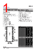
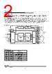

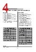
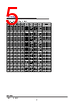



1. I2C Communication Overview
️· Purpose: The I2C interface is used to control various features of the chip, primarily frequency selection and output enabling/disabling.
️· Registers: Control is achieved by writing data to specific registers via the I2C bus. Several registers are defined to control different aspects of the chip's functionality.
2. Key Registers and Control Functions
️· Byte 0: Frequency Select Register:
- FS Source (Bit 7): Selects the source of the frequency control (Hardware IIC or other).
- SS_EN (Bit 6): Enables/disables spread spectrum control.
- SEL12/48MHz (Bit 5): Selects between 12MHz and 48MHz output.
- FS4-FS0 (Bits 4-0): These bits combine to form a frequency selection code based on the "Frequency Selection Table" (Table 1).
️· Byte 1: Output Control Register:
- 24_48MHz (Bit 7): Enables/Disables 24/48MHz output.
- 48MHz (Bit 6): Enables/Disables 48MHz output.
- SEL24/48MHz (Bit 5): Selects between 24MHz and 48MHz output.
- IOAPIC1, IOAPIC0 (Bits 4, 3): Enables/disables the IOAPIC1 and IOAPIC0 outputs.
- CPUCLKODT1, CPUCLKODT0 (Bits 1, 0): Enables/disables the CPU Clock outputs.
️· Byte 2: Output Control Register:
- PCICLK_F1 - PCICLK0 (Bits 7-0): Enables/disables several PCI Clock outputs.
️· Byte 3: Output Control Register:
- REF2 - REF0 (Bits 7-5): Enables/disables reference clock outputs.
- ZCLK1, ZCLK0 (Bits 3, 2): Enables/disables ZCLK outputs.
- AGPCLK1, AGPCLK0 (Bits 1, 0): Enables/disables AGP Clock outputs.
3. Frequency Selection
️· The device uses a combination of the `FS4-FS0` bits (in Byte 0) and potentially other settings to select a specific frequency. The frequencies are defined in Table 1: Frequency Selection Table (not provided in the text but is referenced).
️· The `SEL12/48MHz` bit enables control between 12MHz and 48MHz outputs.
4. Output Control
️· Each output pin (e.g., PCICLK0, AGPCLK0, REF0) has a corresponding enable/disable bit in the appropriate Output Control Register.
️· By writing to these bits, you can individually control whether each output pin is active.
️· Create a table summarizing all the output pins and their corresponding control bits.
️· Explain the potential use cases for the frequency selection options.
️· Explain the role of the spread spectrum control.
️· Help you understand the bit patterns needed to achieve specific configurations.
1. I2C Communication Overview
️· Purpose: The I2C interface is used to control various features of the chip, primarily frequency selection and output enabling/disabling.
️· Registers: Control is achieved by writing data to specific registers via the I2C bus. Several registers are defined to control different aspects of the chip's functionality.
2. Key Registers and Control Functions
️· Byte 0: Frequency Select Register:
- FS Source (Bit 7): Selects the source of the frequency control (Hardware IIC or other).
- SS_EN (Bit 6): Enables/disables spread spectrum control.
- SEL12/48MHz (Bit 5): Selects between 12MHz and 48MHz output.
- FS4-FS0 (Bits 4-0): These bits combine to form a frequency selection code based on the "Frequency Selection Table" (Table 1).
️· Byte 1: Output Control Register:
- 24_48MHz (Bit 7): Enables/Disables 24/48MHz output.
- 48MHz (Bit 6): Enables/Disables 48MHz output.
- SEL24/48MHz (Bit 5): Selects between 24MHz and 48MHz output.
- IOAPIC1, IOAPIC0 (Bits 4, 3): Enables/disables the IOAPIC1 and IOAPIC0 outputs.
- CPUCLKODT1, CPUCLKODT0 (Bits 1, 0): Enables/disables the CPU Clock outputs.
️· Byte 2: Output Control Register:
- PCICLK_F1 - PCICLK0 (Bits 7-0): Enables/disables several PCI Clock outputs.
️· Byte 3: Output Control Register:
- REF2 - REF0 (Bits 7-5): Enables/disables reference clock outputs.
- ZCLK1, ZCLK0 (Bits 3, 2): Enables/disables ZCLK outputs.
- AGPCLK1, AGPCLK0 (Bits 1, 0): Enables/disables AGP Clock outputs.
3. Frequency Selection
️· The device uses a combination of the `FS4-FS0` bits (in Byte 0) and potentially other settings to select a specific frequency. The frequencies are defined in Table 1: Frequency Selection Table (not provided in the text but is referenced).
️· The `SEL12/48MHz` bit enables control between 12MHz and 48MHz outputs.
4. Output Control
️· Each output pin (e.g., PCICLK0, AGPCLK0, REF0) has a corresponding enable/disable bit in the appropriate Output Control Register.
️· By writing to these bits, you can individually control whether each output pin is active.
️· Create a table summarizing all the output pins and their corresponding control bits.
️· Explain the potential use cases for the frequency selection options.
️· Explain the role of the spread spectrum control.
️· Help you understand the bit patterns needed to achieve specific configurations.
| Part No. | ICS952702 |
| Manufacturer | RENESAS |
| Size | 340 Kbytes |
| Pages | 18 pages |
| Description | Programmable Timing Control Hub for K7TM System |
| ALLDATASHEET vous a-t-il été utile ? [ DONATE ] |
À propos de Alldatasheet | Publicité | Contactez-nous | Politique de confidentialité | Lien vers la fiche technique | Echange de liens | Fabricants All Rights Reserved©Alldatasheet.com |
| Russian : Alldatasheetru.com | Korean : Alldatasheet.co.kr | Spanish : Alldatasheet.es | French : Alldatasheet.fr | Italian : Alldatasheetit.com Portuguese : Alldatasheetpt.com | Polish : Alldatasheet.pl | Vietnamese : Alldatasheet.vn Indian : Alldatasheet.in | Mexican : Alldatasheet.com.mx | British : Alldatasheet.co.uk | New Zealand : Alldatasheet.co.nz |
|
Family Site : ic2ic.com |
icmetro.com |
 French ▼
  English
 Chinese
 German
 Japanese
 Russian
 Korean
 Spanish
 Italian
 Portuguese
 Polish
 Vietnamese
 Indian
 Mexican
 British
 New Zealand