 |
Moteur de recherche de fiches techniques de composants électroniques |
|
|
Moteur de recherche de fiches techniques de composants électroniques |
|
The question interval is too short.
Please try again in a few seconds.

Hello, Please ask a question about DP8406 Datasheet
# Example questions:
➢ In diagnostic mode, what does the document state happens to the check word and data input latch, and what is the purpose of this configuration?
➢ What must happen to the check word when a byte is altered during this process?
➢ What are the two error flags and what does it indicate when each is set low?
| Part No. | DP8406 |
| Manufacturer | NSC |
| Size | 225 Kbytes |
| Pages | 14 pages |
| Description | 32-Bit Parallel Error Detection and Correction Circuit |

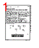
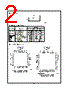
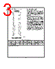
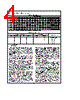
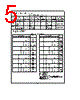
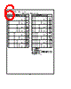
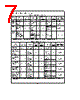
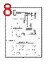
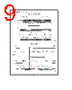

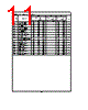
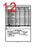
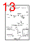


This is a complex excerpt from a technical document, likely a datasheet for a memory error correction and detection (EDAC) chip, the 'F632'. Here's a breakdown of the key information, summarizing it for clarity:
1. Core Functionality - EDAC (Error Detection & Correction):
️· The 'F632' chip is designed to detect and, in many cases, correct single-bit errors in 32-bit memory words, along with providing error flags to indicate the error type.
️· Error Flags:
- ERR (Single Error): Low when a single-bit error is detected and corrected.
- MERR (Multiple Errors): Low when two or more bits are in error. (Correction fails)
️· Limitations:
- 2-bit Errors: EDAC can't correct these; both error flags go LOW.
- 3+ Bit Errors: Can lead to incorrect results - the chip might falsely detect a correctable error or an uncorrectable error.
- Gross Error Conditions: Detects scenarios where all bits are high or all bits are low.
2. Read-Modify-Write (Byte Control) Operations:
️· Allows modifications to individual bytes within a 39-bit memory word.
️· Requires latching data into input latches first.
️· OEB control signals are used to enable or disable specific bytes for modification.
3. Diagnostic Operations:
️· The chip includes diagnostic features to verify its own functionality and memory integrity.
️· Diagnostic Modes: Allows testing with known data patterns.
️· Verification: Testing error flags and syndrome output to locate bad memory locations.
4. Key Terminology:
️· S1, S0: Control signals used to select various operating modes (read, flag, latch, correction, diagnostic).
️· OEB0-OEB3: Output Enable signals controlling individual bytes.
️· CB0-CB6: Check Word Output Ports displaying error codes (syndromes).
️· LED BO: signal for latching a byte.
️· OECB: signal to output the check word.
Overall, the document describes a sophisticated memory error management chip with features for correction, byte-level modifications, and comprehensive diagnostics.
This is a complex excerpt from a technical document, likely a datasheet for a memory error correction and detection (EDAC) chip, the 'F632'. Here's a breakdown of the key information, summarizing it for clarity:
1. Core Functionality - EDAC (Error Detection & Correction):
️· The 'F632' chip is designed to detect and, in many cases, correct single-bit errors in 32-bit memory words, along with providing error flags to indicate the error type.
️· Error Flags:
- ERR (Single Error): Low when a single-bit error is detected and corrected.
- MERR (Multiple Errors): Low when two or more bits are in error. (Correction fails)
️· Limitations:
- 2-bit Errors: EDAC can't correct these; both error flags go LOW.
- 3+ Bit Errors: Can lead to incorrect results - the chip might falsely detect a correctable error or an uncorrectable error.
- Gross Error Conditions: Detects scenarios where all bits are high or all bits are low.
2. Read-Modify-Write (Byte Control) Operations:
️· Allows modifications to individual bytes within a 39-bit memory word.
️· Requires latching data into input latches first.
️· OEB control signals are used to enable or disable specific bytes for modification.
3. Diagnostic Operations:
️· The chip includes diagnostic features to verify its own functionality and memory integrity.
️· Diagnostic Modes: Allows testing with known data patterns.
️· Verification: Testing error flags and syndrome output to locate bad memory locations.
4. Key Terminology:
️· S1, S0: Control signals used to select various operating modes (read, flag, latch, correction, diagnostic).
️· OEB0-OEB3: Output Enable signals controlling individual bytes.
️· CB0-CB6: Check Word Output Ports displaying error codes (syndromes).
️· LED BO: signal for latching a byte.
️· OECB: signal to output the check word.
Overall, the document describes a sophisticated memory error management chip with features for correction, byte-level modifications, and comprehensive diagnostics.
| Part No. | DP8406 |
| Manufacturer | NSC |
| Size | 225 Kbytes |
| Pages | 14 pages |
| Description | 32-Bit Parallel Error Detection and Correction Circuit |
| ALLDATASHEET vous a-t-il été utile ? [ DONATE ] |
À propos de Alldatasheet | Publicité | Contactez-nous | Politique de confidentialité | Lien vers la fiche technique | Echange de liens | Fabricants All Rights Reserved©Alldatasheet.com |
| Russian : Alldatasheetru.com | Korean : Alldatasheet.co.kr | Spanish : Alldatasheet.es | French : Alldatasheet.fr | Italian : Alldatasheetit.com Portuguese : Alldatasheetpt.com | Polish : Alldatasheet.pl | Vietnamese : Alldatasheet.vn Indian : Alldatasheet.in | Mexican : Alldatasheet.com.mx | British : Alldatasheet.co.uk | New Zealand : Alldatasheet.co.nz |
|
Family Site : ic2ic.com |
icmetro.com |
 French ▼
  English
 Chinese
 German
 Japanese
 Russian
 Korean
 Spanish
 Italian
 Portuguese
 Polish
 Vietnamese
 Indian
 Mexican
 British
 New Zealand