 |
Moteur de recherche de fiches techniques de composants électroniques |
|
|
Moteur de recherche de fiches techniques de composants électroniques |
|
The question interval is too short.
Please try again in a few seconds.

Hello, Please ask a question about LTC2381-16 Datasheet
# Example questions:
➢ What is the typical power dissipation of the ltc2381-16 at a sampling rate of 250ksps?
➢ Explain the function of the 'chain' pin and how it affects the operation of the rdl/sdi pin.
➢ What are the acceptable voltage ranges for vdd and ref?
| Part No. | LTC2381-16 |
| Manufacturer | LINER |
| Size | 1Mb |
| Pages | 24 pages |
| Description | 16-Bit, 250ksps, Low Power SAR ADC with Serial Interface |

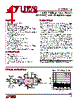





1. Overview: LTC2381-16 – 16-Bit ADC
️· Type: Successive Approximation Register (SAR) Analog-to-Digital Converter (ADC)
️· Resolution: 16-bit
️· Differential Input Range: ±2.5V
️· Sampling Rate: Up to 250ksps (kilosamples per second)
️· Supply Voltage (Vdd): 2.375V - 2.625V
️· Reference Voltage (Vref): 2.4V - 2.6V
️· Power Consumption: Low, with auto power-down feature. Approximately 3.25mW at 250ksps.
️· Applications: High-performance data acquisition, precision measurement, instrumentation.
2. Key Features & Benefits
️· High Accuracy: ±2 LSB INL (Integral Non-Linearity) max, no missing codes.
️· Noise Performance: 92dB SNR (Signal-to-Noise Ratio).
️· Fast Throughput: 250ksps with no cycle latency.
️· Extended Acquisition Time: 3.25µs, allows the use of low-power ADC drivers.
️· Flexible Interface: Serial interface for data output.
️· Daisychain Capability: Chain mode functionality (via CHAIN pin) for multiple ADC connections.
️· Power Optimization: Auto power-down for reduced power consumption when inactive.
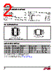
3. Pin Functions
| Pin | Function | Description |
|---|---|---|
| CHAIN | Chain Mode Selector/Serial Data Input | Selects Normal (RDL/SDI as enable) or Chain mode (SDI input). |
| Vdd | Digital Power Supply (Positive) | 2.375V - 2.625V. Requires 10µF bypass capacitor to GND. |
| GND | Ground | Multiple ground pins. Connect to ground plane. |
| IN+ | Positive Differential Analog Input | Differential input, connected to analog signal. |
| IN- | Negative Differential Analog Input | Differential input, connected to reference/inverted analog signal. |
| REF | Reference Input | 2.4V - 2.6V. Requires 47µF ceramic capacitor to GND. |
| CNV | Convert Input | Rising edge initiates conversion. Holding CNV high keeps the part powered down. |
| BUSY | Busy Indicator | High during conversion, low when finished. |
| RDL/SDI | Bus Enable/Serial Data Input | Function depends on CHAIN pin state. |
| SCK | Serial Data Clock Input | Clock for serial data output (or input in Chain mode). |
| SDO | Serial Data Output | Serial data output. Data is 2's complement format. |
| VddIO | Digital I/O Power Supply (Positive) | 1.71V - 5.25V. Requires 0.1µF capacitor to GND. Nominally matches host interface supply. |
| GND (Exposed Pad) | Ground | For DFN package only. Must be soldered to ground plane. |
1. Overview: LTC2381-16 – 16-Bit ADC
️· Type: Successive Approximation Register (SAR) Analog-to-Digital Converter (ADC)
️· Resolution: 16-bit
️· Differential Input Range: ±2.5V
️· Sampling Rate: Up to 250ksps (kilosamples per second)
️· Supply Voltage (Vdd): 2.375V - 2.625V
️· Reference Voltage (Vref): 2.4V - 2.6V
️· Power Consumption: Low, with auto power-down feature. Approximately 3.25mW at 250ksps.
️· Applications: High-performance data acquisition, precision measurement, instrumentation.
2. Key Features & Benefits
️· High Accuracy: ±2 LSB INL (Integral Non-Linearity) max, no missing codes.
️· Noise Performance: 92dB SNR (Signal-to-Noise Ratio).
️· Fast Throughput: 250ksps with no cycle latency.
️· Extended Acquisition Time: 3.25µs, allows the use of low-power ADC drivers.
️· Flexible Interface: Serial interface for data output.
️· Daisychain Capability: Chain mode functionality (via CHAIN pin) for multiple ADC connections.
️· Power Optimization: Auto power-down for reduced power consumption when inactive.
3. Pin Functions
| Pin | Function | Description |
|---|---|---|
| CHAIN | Chain Mode Selector/Serial Data Input | Selects Normal (RDL/SDI as enable) or Chain mode (SDI input). |
| Vdd | Digital Power Supply (Positive) | 2.375V - 2.625V. Requires 10µF bypass capacitor to GND. |
| GND | Ground | Multiple ground pins. Connect to ground plane. |
| IN+ | Positive Differential Analog Input | Differential input, connected to analog signal. |
| IN- | Negative Differential Analog Input | Differential input, connected to reference/inverted analog signal. |
| REF | Reference Input | 2.4V - 2.6V. Requires 47µF ceramic capacitor to GND. |
| CNV | Convert Input | Rising edge initiates conversion. Holding CNV high keeps the part powered down. |
| BUSY | Busy Indicator | High during conversion, low when finished. |
| RDL/SDI | Bus Enable/Serial Data Input | Function depends on CHAIN pin state. |
| SCK | Serial Data Clock Input | Clock for serial data output (or input in Chain mode). |
| SDO | Serial Data Output | Serial data output. Data is 2's complement format. |
| VddIO | Digital I/O Power Supply (Positive) | 1.71V - 5.25V. Requires 0.1µF capacitor to GND. Nominally matches host interface supply. |
| GND (Exposed Pad) | Ground | For DFN package only. Must be soldered to ground plane. |
| Part No. | LTC2381-16 |
| Manufacturer | LINER |
| Size | 1Mb |
| Pages | 24 pages |
| Description | 16-Bit, 250ksps, Low Power SAR ADC with Serial Interface |
| ALLDATASHEET vous a-t-il été utile ? [ DONATE ] |
À propos de Alldatasheet | Publicité | Contactez-nous | Politique de confidentialité | Lien vers la fiche technique | Echange de liens | Fabricants All Rights Reserved©Alldatasheet.com |
| Russian : Alldatasheetru.com | Korean : Alldatasheet.co.kr | Spanish : Alldatasheet.es | French : Alldatasheet.fr | Italian : Alldatasheetit.com Portuguese : Alldatasheetpt.com | Polish : Alldatasheet.pl | Vietnamese : Alldatasheet.vn Indian : Alldatasheet.in | Mexican : Alldatasheet.com.mx | British : Alldatasheet.co.uk | New Zealand : Alldatasheet.co.nz |
|
Family Site : ic2ic.com |
icmetro.com |
 French ▼
  English
 Chinese
 German
 Japanese
 Russian
 Korean
 Spanish
 Italian
 Portuguese
 Polish
 Vietnamese
 Indian
 Mexican
 British
 New Zealand