 |
Moteur de recherche de fiches techniques de composants électroniques |
|
|
Moteur de recherche de fiches techniques de composants électroniques |
|
The question interval is too short.
Please try again in a few seconds.

Hello, Please ask a question about AS1536-BSOU Datasheet
# Example questions:
➢ What is the primary difference in functionality between the as1536 and the as1537?
➢ Describe the process of initiating a conversion and reading the digital output from the as1536/as1537, detailing the roles of the csn and sclk pins.
➢ What factors influence the acquisition time (tacq) and how can it be minimized?
| Part No. | AS1536-BSOU |
| Manufacturer | AMSCO |
| Size | 782 Kbytes |
| Pages | 21 pages |
| Description | 12-Bit, Single Supply, Low-Power, 73ksps A/D Converters |


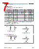
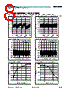
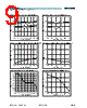
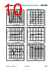


1. Overview & Function
️· What they are: Analog-to-Digital Converters (ADCs)
️· Resolution: 12-bit
️· Modes of Operation:
- Normal A/D Conversion Mode: Active mode, converts analog signals.
- Shutdown Mode: Reduces power consumption (SHDNN pin pulled low).
️· Input Range: 0V to VREF (typically 2.5V)
️· Interface: Simple 3-line serial interface (SCLK, CSN, DOUT) for microprocessor connection.
️· Key Features:
- Integrated track/hold circuitry (no external capacitor needed).
- No external clock required - allows for flexible data read timing.
- Internal Reference: AS1536 has an internal reference (2.5V); AS1537 requires external.
- Input protection diodes to prevent damage from overvoltage.
2. Electrical Characteristics & Timing
️· Conversion Time: 13.7µs (includes track/hold acquisition time).
️· Input Source Impedance: Affects conversion time (tACQ). Higher impedance requires longer acquisition.
️· Minimum Acquisition Time (tACQ): Should be > 1.5µs.
️· Timing Sequence (important for serial data transfer):
- Falling edge of CSN initiates conversion.
- DOUT goes low and stays low until conversion is complete.
- Rising edge of DOUT signals conversion complete (framing signal).
- 13 falling clock edges (SCLK) required to shift out 12 data bits + 1 leading bit.
️· Shutdown Features:
- Significant power savings in shutdown mode.
- Wake-up time (tWAKE) depends on reference capacitor discharge time (AS1536).
3. Key Operation Details
️· Track/Hold Circuit: Samples the analog input voltage, and holds it for conversion.
️· Input Protection: Diodes protect the input from excessive voltage but might affect accuracy near the voltage extremes.
️· Serial Data Output: Unipolar data, output is binary.
️· Transfer Function: Code transitions midway between LSB values. 1 LSB is approximately 610µV when VREF is 2.5V.
4. Power Management
️· Reducing Supply Current: Utilize shutdown mode when not actively converting.
️· Wake-up Time: Consider wake-up time (tWAKE) when designing power-saving strategies.
5. Summary Table (Key Specs)
| Feature | AS1536 | AS1537 |
|---|---|---|
| Resolution | 12-bit | 12-bit |
| Reference | Internal (2.5V) | External |
| Conversion Time | 13.7µs | 13.7µs |
| Interface | Serial (3-wire) | Serial (3-wire) |
| Power Saving | Shutdown mode | Shutdown mode |
1. Overview & Function
️· What they are: Analog-to-Digital Converters (ADCs)
️· Resolution: 12-bit
️· Modes of Operation:
- Normal A/D Conversion Mode: Active mode, converts analog signals.
- Shutdown Mode: Reduces power consumption (SHDNN pin pulled low).
️· Input Range: 0V to VREF (typically 2.5V)
️· Interface: Simple 3-line serial interface (SCLK, CSN, DOUT) for microprocessor connection.
️· Key Features:
- Integrated track/hold circuitry (no external capacitor needed).
- No external clock required - allows for flexible data read timing.
- Internal Reference: AS1536 has an internal reference (2.5V); AS1537 requires external.
- Input protection diodes to prevent damage from overvoltage.
2. Electrical Characteristics & Timing
️· Conversion Time: 13.7µs (includes track/hold acquisition time).
️· Input Source Impedance: Affects conversion time (tACQ). Higher impedance requires longer acquisition.
️· Minimum Acquisition Time (tACQ): Should be > 1.5µs.
️· Timing Sequence (important for serial data transfer):
- Falling edge of CSN initiates conversion.
- DOUT goes low and stays low until conversion is complete.
- Rising edge of DOUT signals conversion complete (framing signal).
- 13 falling clock edges (SCLK) required to shift out 12 data bits + 1 leading bit.
️· Shutdown Features:
- Significant power savings in shutdown mode.
- Wake-up time (tWAKE) depends on reference capacitor discharge time (AS1536).
3. Key Operation Details
️· Track/Hold Circuit: Samples the analog input voltage, and holds it for conversion.
️· Input Protection: Diodes protect the input from excessive voltage but might affect accuracy near the voltage extremes.
️· Serial Data Output: Unipolar data, output is binary.
️· Transfer Function: Code transitions midway between LSB values. 1 LSB is approximately 610µV when VREF is 2.5V.
4. Power Management
️· Reducing Supply Current: Utilize shutdown mode when not actively converting.
️· Wake-up Time: Consider wake-up time (tWAKE) when designing power-saving strategies.
5. Summary Table (Key Specs)
| Feature | AS1536 | AS1537 |
|---|---|---|
| Resolution | 12-bit | 12-bit |
| Reference | Internal (2.5V) | External |
| Conversion Time | 13.7µs | 13.7µs |
| Interface | Serial (3-wire) | Serial (3-wire) |
| Power Saving | Shutdown mode | Shutdown mode |
| Part No. | AS1536-BSOU |
| Manufacturer | AMSCO |
| Size | 782 Kbytes |
| Pages | 21 pages |
| Description | 12-Bit, Single Supply, Low-Power, 73ksps A/D Converters |
| ALLDATASHEET vous a-t-il été utile ? [ DONATE ] |
À propos de Alldatasheet | Publicité | Contactez-nous | Politique de confidentialité | Lien vers la fiche technique | Echange de liens | Fabricants All Rights Reserved©Alldatasheet.com |
| Russian : Alldatasheetru.com | Korean : Alldatasheet.co.kr | Spanish : Alldatasheet.es | French : Alldatasheet.fr | Italian : Alldatasheetit.com Portuguese : Alldatasheetpt.com | Polish : Alldatasheet.pl | Vietnamese : Alldatasheet.vn Indian : Alldatasheet.in | Mexican : Alldatasheet.com.mx | British : Alldatasheet.co.uk | New Zealand : Alldatasheet.co.nz |
|
Family Site : ic2ic.com |
icmetro.com |
 French ▼
  English
 Chinese
 German
 Japanese
 Russian
 Korean
 Spanish
 Italian
 Portuguese
 Polish
 Vietnamese
 Indian
 Mexican
 British
 New Zealand